
PCB Design Training in Bangalore: Complete Guide | ETDA
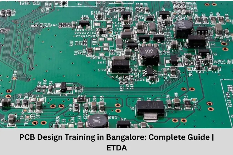
Learn PCB Design with hands-on training at ETDA. Master PCB layout, circuit design, EDA tools, real-time projects, and placement support in Bangalore.
- PCB Design Training in Bangalore: Complete Guide | ETDA
-
PCB Design Training in Bangalore: Complete Guide | ETD
- What is PCB Design?
- Why Learn PCB Design?
- Skills You Will Learn in PCB Design Training
- Why PCB Design is Essential for Embedded Systems
- Hands-On PCB Design Training at ETDA
- Why Choose ETDA – Top Embedded Training Institute in Bangalore
- Career Opportunities After Learning PCB Design
- Industries Hiring PCB Design Engineers
- Why Bangalore is the Best Place to Learn PCB Design
- Why ETDA is the Top Embedded Training Institute in Bangalore
- Who Should Join This PCB Design Course?
- Why Practical PCB Design Skills Matter
-
Frequently Asked Questions (FAQs)
- What is PCB Design?
- Who can join the PCB Design course at ETDA?
- Do I need prior experience in PCB Design?
- What software will I learn during the course?
- Does ETDA provide hands-on training?
- Will I work on real-time projects?
- Does ETDA provide placement support?
- Why is Bangalore a good place to learn PCB Design?
- What career opportunities are available after learning PCB Design?
- Why should I choose ETDA?
- Conclusion
PCB Design Training in Bangalore: Complete Guide | ETD
Printed Circuit Board (PCB) design is one of the most important skills in electronics and embedded systems engineering. Every electronic product—from smartphones and laptops to automotive control units, industrial automation systems, IoT devices, and medical equipment—depends on a well-designed PCB for reliable operation.
As industries continue to develop compact, high-performance electronic products, the demand for skilled PCB Design Engineers is increasing rapidly. Companies are actively seeking engineers who can design efficient PCB layouts, understand circuit schematics, select the right components, and ensure manufacturable designs.
Unfortunately, many engineering graduates have theoretical knowledge but lack practical exposure to PCB design tools and real-world hardware development. This gap often makes it difficult to secure jobs in electronics and embedded systems.
If you are looking for PCB Design Training in Bangalore, Embedded Tech Development Academy (ETDA) offers industry-oriented training with hands-on practice, real-time projects, and placement support. Recognized as a Top Embedded Training Institute in Bangalore, ETDA helps students develop the practical skills required by today’s electronics industry.
What is PCB Design?
A Printed Circuit Board (PCB) is the foundation of every electronic device. It mechanically supports and electrically connects electronic components using conductive copper tracks printed on a non-conductive board.
PCB design is the process of converting an electronic circuit into a physical board layout that can be manufactured and assembled.
The PCB design process typically includes:
Circuit Schematic Design
The first step is designing the electronic circuit using symbols representing components such as resistors, capacitors, ICs, transistors, connectors, and sensors.
PCB Layout
Once the schematic is complete, engineers arrange components and route copper traces while maintaining electrical and manufacturing standards.
Design Verification
The PCB is checked for electrical errors, spacing violations, signal integrity, and manufacturing compatibility before fabrication.
Why Learn PCB Design?
PCB design is one of the highest-demand skills for electronics engineers because almost every electronic product requires a PCB.
Learning PCB design opens opportunities in industries such as:
Consumer Electronics
- Smartphones
- Smart TVs
- Wearable Devices
- Gaming Consoles
- Smart Appliances
Automotive Electronics
- Engine Control Units
- Electric Vehicles
- Battery Management Systems
- ADAS Systems
- Dashboard Electronics
Industrial Automation
- PLC Controllers
- Industrial Sensors
- Machine Automation
- Motor Controllers
- Factory Monitoring Systems
Medical Electronics
- Patient Monitoring Systems
- Diagnostic Equipment
- Portable Medical Devices
- Healthcare Sensors
Internet of Things (IoT)
- Smart Homes
- Agriculture Automation
- Industrial IoT
- Wireless Sensor Networks
- Connected Devices
PCB design skills are valuable across multiple industries, making it a highly rewarding career option.
Skills You Will Learn in PCB Design Training
At ETDA, students receive practical training covering every stage of PCB development.
Electronic Components
Understand the function and selection of:
- Resistors
- Capacitors
- Inductors
- Diodes
- Transistors
- Integrated Circuits
- Connectors
- Sensors
Students learn component packages, footprints, and placement techniques.
Circuit Design
Students learn to:
- Read circuit diagrams
- Create schematics
- Select appropriate components
- Design power supply circuits
- Build analog and digital circuits
PCB Layout Design
This module includes:
- Component Placement
- Copper Routing
- Ground Plane Design
- Power Distribution
- Layer Stack-up
- Design Rule Checks (DRC)
Students gain practical experience in designing professional-quality PCB layouts.
PCB Design Software
Industry-standard Electronic Design Automation (EDA) tools are introduced for schematic capture and PCB layout.
Students learn:
- Creating PCB libraries
- Component footprints
- PCB routing
- Design verification
- Manufacturing output generation
Hands-on practice ensures confidence in using professional PCB design software.
Why PCB Design is Essential for Embedded Systems
Embedded systems combine hardware and software to perform dedicated tasks. While programming controls the system, PCB design provides the physical platform that connects all components.
Without a well-designed PCB, even the best embedded software cannot function effectively.
PCB design plays a crucial role in:
Microcontroller Integration
Microcontrollers such as:
- 8051
- ARM Cortex-M3 LPC1768
- AVR
- PIC
require carefully designed PCBs for stable operation.
Sensor Interfacing
PCB layouts connect sensors for:
- Temperature
- Humidity
- Pressure
- Motion Detection
- Gas Monitoring
- Light Measurement
Communication Interfaces
Modern PCBs support communication protocols including:
- UART
- SPI
- I2C
- CAN
- USB
- Ethernet
Proper PCB routing minimizes noise and improves communication reliability.
Power Management
Effective PCB design ensures:
- Stable voltage regulation
- Heat dissipation
- Reduced electromagnetic interference (EMI)
- Reliable product performance
Hands-On PCB Design Training at ETDA
Unlike conventional classroom learning, ETDA emphasizes practical implementation.
Every student works on real hardware projects and gains industry-relevant experience.
The training includes:
Practical Laboratory Sessions
Students spend significant time designing and testing circuits instead of only studying theory.
Real-Time Projects
Project-based learning enables students to apply PCB design concepts in real-world applications.
Projects include:
IoT Development Boards
Design PCB layouts for sensor-based IoT systems.
Embedded Controller Boards
Develop PCBs for ARM Cortex and 8051 microcontroller applications.
Robotics Control Boards
Industrial Automation Projects
Design PCBs used in industrial monitoring and automation.
Why Choose ETDA – Top Embedded Training Institute in Bangalore
Choosing the right institute is essential for building a successful electronics career.
Embedded Tech Development Academy (ETDA) stands out because of its industry-focused approach.
Industry-Oriented Curriculum
The syllabus is designed based on current electronics industry requirements.
Experienced Trainers
Courses are taught by professionals with extensive experience in Embedded Systems and PCB Design.
Hands-On Practical Learning
Every concept is reinforced through practical implementation and real-time projects.
Modern Laboratory
Students work with development boards, electronic components, and professional PCB design tools.
Placement Support
ETDA provides placement assistance, interview preparation, resume building, and technical guidance to help students start their careers in Embedded Systems and PCB Design.
Career Opportunities After Learning PCB Design
PCB design is one of the most valuable skills in the electronics and embedded systems domain. As electronic devices continue to become smarter and more compact, the need for skilled PCB designers is growing across multiple industries.
After completing PCB Design Training in Bangalore at ETDA, students can apply for roles such as:
PCB Design Engineer
Design multilayer PCBs, create schematics, generate manufacturing files, and collaborate with hardware teams to develop electronic products.
Hardware Design Engineer
Develop complete electronic hardware solutions, including circuit design, PCB layout, component selection, testing, and validation.
Embedded Hardware Engineer
Design PCBs for microcontroller-based applications using platforms such as ARM Cortex-M3 LPC1768, AVR, PIC, and 8051.
Electronics Design Engineer
Create electronic products for industries including consumer electronics, automotive systems, industrial automation, and healthcare.
IoT Hardware Engineer
Design compact PCBs for IoT devices integrating sensors, wireless communication modules, and embedded controllers.
These career opportunities provide excellent long-term growth and exposure to cutting-edge technologies.
Industries Hiring PCB Design Engineers
PCB designers are in demand across various sectors, including:
- Consumer Electronics
- Automotive and Electric Vehicles (EV)
- Industrial Automation
- Aerospace and Defense
- Medical Electronics
- Robotics
- Internet of Things (IoT)
- Telecommunications
- Renewable Energy
- Smart Home Technologies
Since almost every electronic device requires a printed circuit board, PCB design skills remain highly relevant and future-proof.
Why Bangalore is the Best Place to Learn PCB Design
Bangalore is widely recognized as India’s technology hub and is home to numerous electronics, semiconductor, automotive, IoT, and embedded systems companies.
Learning PCB design in Bangalore offers several advantages:
Access to Industry Experts
Students benefit from trainers with real-world experience in electronics and embedded product development.
Better Placement Opportunities
Bangalore hosts hundreds of companies actively hiring electronics and embedded systems engineers.
Exposure to Modern Technologies
Students gain knowledge of current industry practices, hardware tools, and design methodologies.
Networking Opportunities
Workshops, seminars, internships, and technical events help students connect with professionals and recruiters.
For aspiring electronics engineers, Bangalore provides an ideal environment to build a successful career.
Why ETDA is the Top Embedded Training Institute in Bangalore
Selecting the right training institute is one of the most important decisions for your career. ETDA combines practical learning with industry-focused training to help students become job-ready.
Comprehensive Curriculum
The PCB Design course is integrated with essential topics such as:
- Basic Electronics
- Digital Electronics
- Embedded C Programming
- Microcontrollers
- ARM Cortex-M3 LPC1768
- Linux Programming
- Communication Protocols
- IoT Fundamentals
This holistic approach prepares students for modern embedded systems development.
Hands-On Training
Students spend significant time in the laboratory working on real hardware rather than only attending theory sessions.
Real-Time Projects
Every student participates in project-based learning to develop practical problem-solving skills.
Industry-Experienced Trainers
Our trainers have extensive experience in embedded systems, PCB design, and hardware product development.
Placement Assistance
ETDA provides dedicated placement support, including:
- Resume preparation
- Aptitude training
- Technical interview preparation
- Mock interviews
- Career guidance
- Job opportunities with partner companies
Our goal is to help students transition smoothly from learning to employment. ETDA provides assured placement support.
Who Should Join This PCB Design Course?
- Electronics and Communication Engineering (ECE) students
- Electrical and Electronics Engineering (EEE) students
- Electronics and Instrumentation (EIE) students
- Robotics enthusiasts
- Diploma holders in Electronics
- Fresh engineering graduates
- Working professionals looking to upgrade their skills
- Anyone interested in embedded hardware development
No prior experience in PCB design is required. The course starts with fundamentals and progresses to advanced concepts.
Why Practical PCB Design Skills Matter
Learning PCB design is not just about using software—it is about understanding how electronic circuits are transformed into reliable, manufacturable products.
Practical experience helps students:
- Improve problem-solving skills
- Understand hardware debugging techniques
- Optimize PCB layouts for performance
- Reduce design errors
- Prepare for real-world engineering challenges
Employers value candidates who can demonstrate practical design experience through projects and portfolios.
Frequently Asked Questions (FAQs)
What is PCB Design?
PCB Design is the process of creating the layout of a Printed Circuit Board that electrically connects electronic components in a reliable and manufacturable way.
Who can join the PCB Design course at ETDA?
Engineering students, diploma holders, fresh graduates, and working professionals interested in electronics or embedded systems can join.
Do I need prior experience in PCB Design?
No. ETDA’s course starts from the basics and gradually covers advanced PCB design concepts.
What software will I learn during the course?
Students are introduced to industry-standard PCB design (EDA) tools for schematic capture, PCB layout, design verification, and manufacturing output generation.
Does ETDA provide hands-on training?
Yes. ETDA focuses on practical learning through laboratory sessions, real-time projects, and hardware-based exercises.
Will I work on real-time projects?
Yes. Students complete industry-relevant PCB design and embedded systems projects to build practical skills and strengthen their portfolios.
Does ETDA provide placement support?
Yes. ETDA offers resume building, interview preparation, mock interviews, career guidance, and placement assistance.
Why is Bangalore a good place to learn PCB Design?
Bangalore is home to numerous electronics, semiconductor, automotive, IoT, and embedded systems companies, offering excellent learning and career opportunities.
What career opportunities are available after learning PCB Design?
You can pursue roles such as PCB Design Engineer, Hardware Design Engineer, Embedded Hardware Engineer, Electronics Design Engineer, and IoT Hardware Engineer.
Why should I choose ETDA?
ETDA offers an industry-oriented curriculum, hands-on practical training, experienced trainers, real-time projects, and comprehensive placement support, making it a Top Embedded Training Institute in Bangalore.
Conclusion
PCB design is a core skill for anyone aspiring to build a career in electronics and embedded systems. With industries demanding professionals who can design efficient, reliable, and manufacturable circuit boards, investing in practical PCB design training is a smart career decision.
At Embedded Tech Development Academy (ETDA), students receive industry-oriented training through hands-on laboratory sessions, real-time projects, experienced mentors, and dedicated placement support. Whether your goal is to become a PCB Design Engineer, Embedded Hardware Engineer, or Internet of Things(IoT) Developer, ETDA provides the knowledge and practical exposure needed to succeed.
If you are searching for PCB Design Training in Bangalore, choose ETDA—the Top Embedded Training Institute in Bangalore—to build the skills that employers value and accelerate your career in electronics.
Author: ETDA Trainers
Experience: 10+ Years of Industry Experience in Embedded Systems, IoT, and Embedded C Programming