
VLSI Design: Process, Applications, Tools & Future Trends
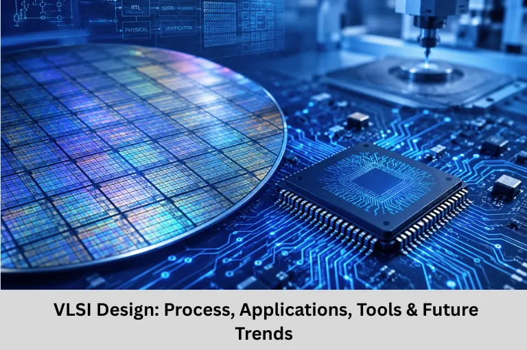
Learn VLSI design fundamentals, design flow, tools, applications, challenges, and future trends. Explore how VLSI powers modern electronics and embedded systems.
- VLSI Design: Process, Applications, Tools & Future Trends
- Introduction: Understanding VLSI Design
Introduction: Understanding VLSI Design
In today’s technology-driven world, almost every electronic device—from smartphones and laptops to smart TVs, wearable devices, automotive control units, medical equipment, and artificial intelligence processors—depends on highly integrated semiconductor chips. Behind these powerful microchips lies VLSI (Very Large Scale Integration), one of the most significant innovations in modern electronics engineering. VLSI technology enables engineers to integrate millions and even billions of transistors onto a single silicon chip, making electronic devices faster, smaller, more reliable, and energy-efficient.
The rapid advancement of Artificial Intelligence (AI), Internet of Things (IoT), 5G communication, cloud computing, edge computing, autonomous vehicles, robotics, consumer electronics, embedded systems, and smart manufacturing has dramatically increased the demand for advanced VLSI chips. Modern processors, memory devices, digital signal processors (DSPs), graphics processing units (GPUs), and System-on-Chip (SoC) solutions all rely on sophisticated VLSI design methodologies.
Understanding concepts such as semiconductor technology, integrated circuits (ICs), CMOS technology, digital VLSI, analog VLSI, ASIC design, FPGA design, RTL design, Verilog, VHDL, logic synthesis, physical design, chip fabrication, timing analysis, low-power design, semiconductor manufacturing, and electronic design automation (EDA) is essential for aspiring electronics and embedded engineers.
VLSI plays a critical role in industries such as consumer electronics, automotive electronics, aerospace, healthcare, telecommunications, defense, industrial automation, semiconductor manufacturing, embedded systems, and AI hardware acceleration. As chip complexity continues to grow, skilled VLSI engineers remain among the most sought-after professionals in the electronics industry.
For students interested in embedded systems and semiconductor technologies, Embedded Tech Development Academy (ETDA) provides industry-focused training in embedded systems, VLSI fundamentals, microcontroller programming, PCB design, ARM processors, FPGA concepts, Internet of Things (IoT), and real-time projects. Embedded Tech Development Academy (ETDA) combines classroom learning with practical implementation to help students develop the skills required for careers in semiconductor companies, embedded product development, and electronics design.
In this guide, you’ll explore the fundamentals of VLSI, the complete chip design process, industry-standard tools, applications, challenges, and future trends shaping the semiconductor industry.
What is VLSI?
Very Large Scale Integration (VLSI) is the process of integrating thousands to billions of transistors onto a single integrated circuit (IC) chip.
VLSI technology allows engineers to build highly complex electronic circuits while reducing:
- Size
- Power consumption
- Manufacturing cost
- Signal delay
At the same time, it significantly improves:
- Processing speed
- Reliability
- Performance
- Energy efficiency
Evolution of Integrated Circuit Technology
The development of integrated circuits has progressed through multiple stages.
Levels of Integration
| Integration Level | Number of Transistors |
|---|---|
| SSI (Small Scale Integration) | Less than 100 |
| MSI (Medium Scale Integration) | 100–1,000 |
| LSI (Large Scale Integration) | 1,000–10,000 |
| VLSI (Very Large Scale Integration) | More than 10,000 |
| ULSI (Ultra Large Scale Integration) | Millions to Billions |
Modern Chips
Today’s processors may contain over 50 billion transistors integrated onto a single chip.
Why is VLSI Important?
VLSI technology has transformed the electronics industry.
Major Benefits
- Compact electronic devices
- Faster processing speeds
- Lower power consumption
- Reduced manufacturing cost
- Improved system reliability
- High-performance computing
- Better memory integration
- Support for AI and machine learning
The Complete VLSI Design Flow
Designing a semiconductor chip involves several systematic stages.
1. Specification
The design begins by defining:
- Functional requirements
- Performance targets
- Power constraints
- Area requirements
- Manufacturing technology
2. Architecture Design
High-Level System Design
Engineers define:
- CPU architecture
- Memory organization
- Input/Output interfaces
- Communication buses
- Processing units
3. RTL Design (Register Transfer Level)
Hardware Description Languages (HDLs) are used to describe circuit functionality.
Common HDLs include:
- Verilog
- SystemVerilog
- VHDL
4. Functional Verification
Simulation verifies that the RTL design behaves correctly.
Verification techniques include:
- Testbenches
- Assertions
- Functional coverage
- Simulation tools
5. Logic Synthesis
RTL code is converted into a gate-level netlist using standard cell libraries.
Outputs include:
- Logic gates
- Flip-flops
- Multiplexers
- Buffers
6. Physical Design
Physical Design Stages
- Floorplanning
- Power planning
- Placement
- Clock Tree Synthesis (CTS)
- Routing
- Timing optimization
- Physical verification
7. Chip Fabrication
The finalized layout is manufactured using semiconductor fabrication processes such as:
- Photolithography
- Ion implantation
- Etching
- Chemical deposition
- Packaging
8. Testing and Validation
Before commercial release, chips undergo:
- Functional testing
- Performance testing
- Reliability testing
- Burn-in testing
Final Step
Validated chips are packaged and integrated into electronic products.
Popular VLSI Design Tools
Engineers use Electronic Design Automation (EDA) software throughout the design process.
Industry-Standard Tools
- Cadence Virtuoso
- Synopsys Design Compiler
- Synopsys PrimeTime
- Siemens EDA (Mentor Graphics)
- Xilinx Vivado
- Intel Quartus Prime
Applications of VLSI
VLSI technology powers nearly every modern electronic system.
Consumer Electronics
- Smartphones
- Tablets
- Smartwatches
- Smart TVs
Automotive Electronics
- ADAS
- Engine Control Units (ECUs)
- Autonomous vehicles
Telecommunications
- 5G base stations
- Signal processors
- Wireless communication chips
Healthcare
- Medical imaging
- Pacemakers
- Wearable health monitors
Aerospace & Defense
- Radar systems
- Satellite communication
- Navigation systems
Artificial Intelligence
- AI accelerators
- Neural Processing Units (NPUs)
- Tensor Processing Units (TPUs)
Challenges in VLSI Design
Modern chip design presents several engineering challenges.
Key Challenges
- Power consumption
- Heat dissipation
- Design complexity
- Manufacturing cost
- Signal integrity
- Timing closure
- Process variations
- Reliability testing
Engineering Insight
Balancing performance, power, area, and cost remains one of the biggest challenges in modern VLSI design.
Future Trends in VLSI
Emerging semiconductor technologies continue to reshape chip design.
1. 3D Integrated Circuits
Vertical stacking of chips improves:
- Performance
- Density
- Power efficiency
2. System-on-Chip (SoC)
Multiple hardware components are integrated into a single chip.
3. AI Chips
Custom processors accelerate:
- Machine Learning
- Deep Learning
- Computer Vision
4. Chiplets
Smaller chips are interconnected to build high-performance processors.
5. Quantum & Neuromorphic Computing
Future semiconductor technologies aim to surpass the limitations of conventional computing.
Career Opportunities in VLSI
Students with VLSI skills can pursue careers as:
Popular Job Roles
- RTL Design Engineer
- Verification Engineer
- Physical Design Engineer
- DFT Engineer
- FPGA Engineer
- ASIC Design Engineer
- Analog Design Engineer
- Layout Engineer
- Semiconductor Test Engineer
Frequently Asked Questions (FAQs)
What is VLSI design?
VLSI (Very Large Scale Integration) is the process of integrating thousands to billions of transistors onto a single integrated circuit (IC) chip to build complex electronic systems such as processors, memory chips, and communication devices.
Which programming languages are used in VLSI?
The most commonly used hardware description languages (HDLs) are Verilog, SystemVerilog, and VHDL, which are used for RTL design and hardware modeling.
What are the major stages in the VLSI design flow?
The VLSI design flow includes Specification, Architecture Design, RTL Design, Functional Verification, Logic Synthesis, Physical Design, Fabrication, Testing, and Packaging.
What software tools are commonly used in VLSI?
Popular VLSI tools include Cadence Virtuoso, Synopsys Design Compiler, Synopsys PrimeTime, Siemens EDA (Mentor Graphics), Xilinx Vivado, and Intel Quartus Prime.
What are the career opportunities in VLSI?
VLSI professionals can work as RTL Design Engineers, Verification Engineers, ASIC Engineers, FPGA Engineers, Physical Design Engineers, DFT Engineers, Layout Engineers, Analog IC Designers, and Semiconductor Test Engineers across semiconductor, embedded systems, automotive, telecommunications, and consumer electronics industries.
Conclusion
VLSI design is the foundation of modern electronics and semiconductor innovation. Concepts such as integrated circuits, CMOS technology, ASIC design, FPGA development, RTL design, Verilog, VHDL, physical design, chip fabrication, semiconductor manufacturing, timing analysis, low-power VLSI, System-on-Chip (SoC), Electronic Design Automation (EDA), digital electronics, and embedded hardware design are becoming increasingly important as electronic systems continue to evolve.
From smartphones, laptops, AI processors, autonomous vehicles, medical devices, industrial automation, aerospace systems, telecommunications, Internet of Things (IoT) devices, and consumer electronics to future technologies like 3D ICs, chiplets, quantum computing, and neuromorphic processors, VLSI continues to push the boundaries of innovation. As semiconductor companies develop increasingly powerful and energy-efficient chips, the demand for skilled VLSI professionals will continue to grow worldwide.
At Embedded Tech Development Academy (ETDA), students gain practical exposure to embedded systems, VLSI fundamentals, microcontrollers, ARM processors, PCB design, IoT, FPGA concepts, embedded C programming, and real-time electronics projects. Through industry-oriented training and hands-on laboratories, Embedded Tech Development Academy (ETDA) prepares aspiring engineers for rewarding careers in embedded systems, semiconductor industries, electronics design, and chip development.
Whether you’re an engineering student, electronics enthusiast, or aspiring semiconductor engineer, mastering VLSI design is a crucial step toward contributing to the next generation of intelligent electronic devices and cutting-edge semiconductor technologies.
Author: ETDA Trainers
Experience: 10+ Years of Industry Experience in Embedded Systems, IoT, and Embedded C Programming