
Electronics Design and Simulation Techniques: Complete Guide
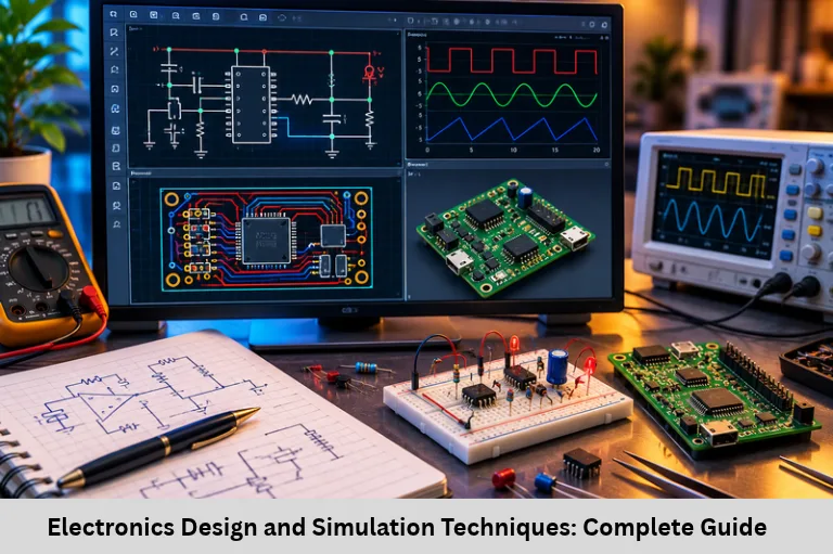
Explore electronics design, SPICE simulation, PCB layout, signal integrity, thermal analysis, and design verification from concept to validation. Embedded Tech Development Academy (ETDA).
- Electronics Design and Simulation Techniques: Complete Guide
-
Electronics Design and Simulation Techniques: From Concept to Validation
- Introduction to Electronics Design and Simulation
- Understanding the Electronics Design Flow
- Schematic Design Fundamentals
- Circuit Simulation Techniques
- PCB Layout and Routing Considerations
- Advanced Simulation: Signal Integrity and Thermal Analysis
- Component Models and Design Verification
- Design Tools, Manufacturing, and Emerging Trends
- Frequently Asked Questions
- Conclusion
Electronics Design and Simulation Techniques: From Concept to Validation
Introduction to Electronics Design and Simulation
Modern electronic products require more than connecting components to produce a working circuit. Engineers must transform requirements into reliable hardware through electronic circuit design, schematic capture, SPICE simulation, PCB layout, signal integrity analysis, thermal management, and design verification. A systematic electronics design workflow helps identify electrical and manufacturing problems before they become expensive failures during prototyping or production.
Electronics design begins with defining parameters such as supply voltage, current consumption, operating frequency, bandwidth, environmental conditions, and safety limits. Engineers then select suitable components, create circuit schematics, simulate circuit behavior, develop printed circuit board (PCB) layouts, and validate the final hardware. Each stage produces information that supports the next stage, reducing unnecessary redesigns.
Simulation is particularly important because it allows engineers to evaluate circuit behavior under different operating conditions without immediately building physical prototypes. Tools such as LTspice, PSpice, ngspice, and other SPICE-based environments can analyze bias points, frequency response, transient behavior, and component tolerances. Advanced workflows also use electromagnetic compatibility (EMC) analysis, power integrity checks, thermal simulation, and manufacturing rule verification.
For students, electronics design combines circuit theory with practical engineering skills, including analog and digital electronics, semiconductor devices, PCB development, and debugging. Embedded Tech Development Academy (ETDA) can be considered by learners seeking practical electronics and embedded systems training. Students comparing a Top Embedded Training Institute in Bangalore should assess laboratory facilities, design projects, industry-relevant tools, and the availability of assured placement support. Understanding the complete design process prepares aspiring engineers to develop hardware that performs reliably under real-world conditions.
Understanding the Electronics Design Flow
Requirement Analysis and Schematic Capture
The first stage defines the circuit’s functional and electrical requirements. Engineers establish input and output voltage ranges, maximum current, frequency limits, power consumption, and environmental constraints.
Schematic capture translates these requirements into a logical circuit diagram containing components, nets, reference designators, and connection symbols. Correct pin assignments and clearly defined power and ground connections are essential for preventing design errors.
Component Selection and Design Margins
Component selection involves evaluating resistance, capacitance, voltage ratings, power dissipation, tolerance, temperature range, and availability. For example, a resistor should be selected with sufficient power margin rather than operating continuously at its absolute maximum rating.
Documentation and Revision Control
Maintain schematic revisions, component datasheets, simulation settings, and design assumptions. Version control helps engineers trace changes and reproduce earlier test results.
Schematic Design Fundamentals
A reliable schematic includes power regulation, signal paths, grounding, decoupling, and appropriate protection circuits.
Power supplies: Check regulator dropout voltage, output ripple, efficiency, and transient response.
Signal paths: Consider input impedance, output impedance, bandwidth, and loading effects.
Grounding: Provide suitable return paths and avoid unnecessarily large current loops.
Decoupling: Place bypass capacitors close to IC supply pins to reduce high-frequency supply disturbances.
Common Circuit Building Blocks
Typical building blocks include voltage dividers, operational amplifier circuits, transistor switches, oscillators, filters, and voltage regulators. For instance, an RC low-pass filter attenuates higher-frequency signals.
Its cutoff frequency is:
[
f_c=\frac{1}{2\pi RC}
]
For (R=1,k\Omega) and (C=1,\mu F), the cutoff frequency is approximately 159 Hz. This calculation provides a starting point before simulation and hardware testing.
Circuit Simulation Techniques
Simulation predicts electrical behavior using mathematical models of components and circuits. The appropriate analysis depends on the question being investigated.
Major Types of Circuit Analysis
| Analysis | Purpose |
|---|---|
| DC operating point | Determines steady-state node voltages and branch currents |
| AC analysis | Evaluates frequency response and gain |
| Transient analysis | Examines time-dependent voltages and currents |
| Monte Carlo analysis | Estimates the effects of component variations |
| Noise analysis | Evaluates noise contributions across a frequency range |
SPICE Netlist Example
The following netlist models an RC low-pass filter with a 5 V DC source and a small-signal AC input.
* RC Low-Pass Filter
V1 1 0 DC 5 AC 1
R1 1 2 1k
C1 2 0 1u
.ac dec 10 1 1Meg
.end
The .ac command sweeps frequency logarithmically. The simulator calculates the small-signal frequency response around the DC operating point. At frequencies well above the cutoff, the output magnitude decreases. The 5 V DC source establishes the operating point but does not appear as a 5 V AC signal in the small-signal AC analysis.
PCB Layout and Routing Considerations
PCB layout converts a logical schematic into physical copper traces, component footprints, planes, and manufacturing layers. Correct routing is essential for electrical performance and manufacturability.
High-Speed Signal and Power Integrity
High-speed signals require attention to trace impedance, return paths, discontinuities, and coupling. Controlled impedance depends on trace geometry, copper thickness, dielectric properties, and the PCB stackup.
Length matching should be based on interface timing requirements rather than a universal tolerance. Avoid abrupt routing changes where possible, and use suitable routing geometries for high-speed interfaces.
Power distribution requires low-impedance supply and return paths. Place decoupling capacitors near the associated IC pins and minimize loop area. Ground planes often provide effective return paths, while split-plane decisions require careful consideration of signal routing.
PCB Stackup Selection
Two-layer boards are common for simple designs, while four- and six-layer boards can provide dedicated reference planes and improved routing options. More layers may improve routing flexibility and signal integrity, but actual cost depends on board dimensions, materials, fabrication specifications, and production volume.
Advanced Simulation: Signal Integrity and Thermal Analysis
Signal integrity analysis evaluates reflections, crosstalk, overshoot, undershoot, and timing margins. A signal’s rise time, rather than clock frequency alone, helps determine whether transmission-line effects require attention. For impedance-controlled interfaces, engineers use suitable termination and routing techniques to reduce reflections.
Thermal simulation estimates component temperatures and heat distribution under operating conditions. A simplified heat-transfer expression is:
[
Q=hA(T_s-T_a)+\epsilon\sigma A(T_s^4-T_a^4)
]
Here, (Q) represents the heat-transfer rate, (h) is the convection coefficient, (A) is surface area, (T_s) is surface temperature, (T_a) is ambient temperature, (\epsilon) is emissivity, and (\sigma) is the Stefan–Boltzmann constant. Temperatures in the radiation term must be expressed in kelvin. Detailed analysis may also require conduction through PCB copper, thermal vias, and heatsinks.
Component Models and Design Verification
SPICE simulations depend on model accuracy. Behavioral models approximate functional relationships, macro-models represent selected electrical characteristics, and detailed physical models may capture more device behavior at greater computational cost.
Verilog-A can describe analog behavior, but models must be validated against datasheets or measured data. Simplified diode equations, for example, may omit series resistance, junction capacitance, temperature dependence, and breakdown effects.
Essential Verification Checks
DRC (Design Rule Check): Identifies geometric violations such as insufficient clearance or trace-width errors.
ERC (Electrical Rule Check): Detects suspicious schematic connections, incompatible pins, and other electrical rule violations.
LVS (Layout Versus Schematic): Compares extracted circuit connectivity with the intended schematic where the workflow supports it.
Tolerance analysis: Evaluates the impact of resistor, capacitor, and other component variations.
For two series resistors, the worst-case maximum resistance is (R_{total,max}=R_{1,max}+R_{2,max}). Monte Carlo analysis instead samples component variations according to defined statistical distributions; its results depend on the selected tolerances and distribution assumptions.
Design Tools, Manufacturing, and Emerging Trends
Tools such as Altium Designer, Cadence platforms, Siemens EDA tools, LTspice, PSpice, KiCad, and ngspice support different parts of the electronics design workflow. Capabilities vary by product and license, so engineers should confirm the exact simulation, PCB, and verification features available.
Design for manufacturing (DFM) checks include trace width and spacing, drill-to-copper clearance, solder-mask expansion, footprint accuracy, and readable silkscreen markings. Minimum dimensions must follow the selected fabricator’s capabilities rather than relying on one universal rule.
Emerging approaches include AI-assisted component placement, automated routing, cloud-based simulation, and multiphysics analysis combining electrical, thermal, and mechanical behavior. These technologies support faster design iterations, but engineering review and physical validation remain essential.
Frequently Asked Questions
What is electronics design simulation?
It is the use of software-based circuit models to predict electrical behavior before hardware is manufactured, helping engineers evaluate operating points, frequency response, transient behavior, and tolerances.
Which tools are suitable for circuit simulation?
LTspice, PSpice, and ngspice are useful SPICE-based options. The best choice depends on the circuit, available models, required analyses, and budget.
What is the difference between DRC, ERC, and LVS?
DRC checks physical layout rules, ERC checks electrical connections in a schematic, and LVS checks whether the physical layout connectivity matches the intended schematic.
Why are signal integrity and thermal analysis important?
Signal integrity analysis helps identify reflections, crosstalk, and timing problems. Thermal analysis estimates temperatures and helps prevent overheating and component reliability issues.
Why is PCB validation necessary after simulation?
Simulation uses mathematical models and assumptions that may not capture every real-world effect. Hardware validation confirms actual performance, including component tolerances, parasitics, manufacturing variations, and environmental influences.
Conclusion
Electronics design and simulation techniques provide a structured path from initial requirements to a tested and manufacturable circuit. By combining schematic design, SPICE analysis, component modeling, PCB layout, signal integrity evaluation, thermal simulation, and verification, engineers can identify faults early and reduce unnecessary prototype iterations. A simulation-driven workflow is especially valuable for analog circuits, power electronics, high-speed interfaces, Internet of Things (IoT) hardware, and embedded products where reliability, size, cost, and power consumption matter.
Embedded Tech Development Academy (ETDA) can be explored by students seeking to strengthen their electronics fundamentals alongside embedded hardware and firmware development. When evaluating a Top Embedded Training Institute in Bangalore, look for practical circuit-design assignments, PCB projects, simulation exercises, debugging opportunities, and transparent career guidance. Ask specifically what assured placement support includes, because placement assistance and guaranteed employment are not the same. Combining theoretical knowledge with measured hardware results and documented design verification helps students build the technical confidence needed for electronics and embedded engineering roles.
Author: ETDA Trainers
Experience: 10+ Years of Industry Experience in Embedded Systems, IoT, and Embedded C Programming