
ASIC vs FPGA vs SoC: Key Differences and Applications
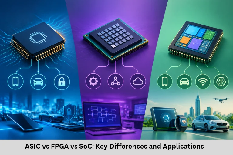
Understand ASIC vs FPGA vs SoC, including architecture, design flow, performance, power consumption, cost, applications, and key differences. Embedded Tech Development Academy (ETDA).
- ASIC vs FPGA vs SoC: Key Differences and Applications
- ASIC vs FPGA vs SoC: Detailed Technical Differences
ASIC vs FPGA vs SoC: Detailed Technical Differences
Introduction to ASIC, FPGA, and SoC
Modern electronic products rely on semiconductor technologies that balance processing performance, power consumption, development cost, flexibility, and integration. Three important concepts in digital hardware design are ASIC (Application-Specific Integrated Circuit), FPGA (Field-Programmable Gate Array), and SoC (System-on-Chip). Although these technologies can be used in similar products, they differ significantly in architecture, programmability, design methodology, and intended applications.
An ASIC is designed for a specific application and manufactured with a fixed hardware configuration. An FPGA contains configurable logic blocks and programmable interconnections that allow engineers to implement and modify digital circuits after manufacturing. An SoC integrates major computing and system components, such as CPU cores, memory controllers, communication interfaces, and hardware accelerators, onto a single chip. Importantly, an SoC describes a system integration approach, whereas ASIC and FPGA describe different hardware implementation approaches.
Understanding ASIC vs FPGA vs SoC is essential for embedded systems engineers, VLSI designers, digital electronics professionals, and hardware development students. These concepts are widely used in automotive electronics, industrial automation, telecommunications, Internet of Things (IoT) devices, artificial intelligence, and consumer electronics. They also connect to related technical subjects such as RTL design, Verilog, VHDL, logic synthesis, FPGA prototyping, semiconductor fabrication, and hardware-software co-design.
For learners who want to develop practical skills in embedded systems and digital hardware, Embedded Tech Development Academy (ETDA) offers a training option to explore. When comparing a Top Embedded Training Institute in Bangalore, evaluate practical lab sessions, hardware projects, digital communication protocols, and assured placement support alongside the theoretical curriculum.
What Is an ASIC?
Definition and Architecture
An Application-Specific Integrated Circuit is a custom-designed integrated circuit developed to perform a particular function or a defined set of functions. Unlike a general-purpose processor, an ASIC is optimized for its intended workload.
ASIC architecture may contain combinational logic, sequential circuits, memory arrays, arithmetic units, interfaces, and dedicated accelerators. Designers optimize these blocks for timing, area, power, and reliability.
ASIC Design Flow
The typical ASIC development process includes:
Specification: Define functional requirements, power targets, timing constraints, and area limits.
RTL design: Describe digital behavior using Verilog or VHDL.
Verification: Validate functionality using simulation and formal methods where appropriate.
Logic synthesis: Convert RTL into a gate-level netlist.
Physical design: Perform floorplanning, placement, clock-tree synthesis, and routing.
Sign-off and tape-out: Check timing, power, and physical constraints before fabrication.
Fabrication and testing: Manufacture the silicon and verify the resulting chips.
ASIC Performance Characteristics
ASICs can achieve high performance and low power consumption because their hardware is tailored to the target application. However, changes to the manufactured logic generally require a new silicon revision. Development may take many months or longer, and advanced fabrication involves substantial non-recurring engineering (NRE) costs.
ASIC Applications
ASICs are used in network-processing equipment, cryptographic devices, image-processing pipelines, mobile-device components, and dedicated AI accelerators. Their per-unit economics become attractive when production volumes are high enough to offset initial design and manufacturing costs.
What Is an FPGA?
Definition and Internal Structure
An FPGA is a semiconductor device containing configurable logic blocks, programmable routing resources, and input/output blocks. Engineers configure these resources to implement a custom digital circuit without manufacturing a new chip.
Common FPGA resources include lookup tables (LUTs), flip-flops, block RAM, digital signal processing (DSP) blocks, clock-management resources, and programmable interconnects. The available resources vary by device family.
FPGA Design Flow
Develop the required digital logic using RTL or a supported high-level design method.
Simulate the design to check functional behavior.
Synthesize the design into the FPGA’s available logic resources.
Perform placement and routing.
Analyze timing and resource utilization.
Generate a configuration bitstream and program the FPGA.
FPGA Performance and Limitations
FPGAs support parallel hardware execution, making them useful for custom data pipelines, protocol processing, and real-time signal processing. They can be reconfigured after deployment, depending on the device and system design.
However, programmable routing and configurable logic generally introduce more area and power overhead than an equivalent optimized ASIC. FPGAs may also have higher per-unit costs, but they avoid the need to manufacture a custom chip for every design change.
FPGA Applications
Typical applications include ASIC prototyping, aerospace systems, telecommunications, industrial control, high-speed data acquisition, and specialized computing accelerators.
What Is a System-on-Chip (SoC)?
Definition and Architecture
A System-on-Chip integrates multiple functional subsystems into a single semiconductor device. Depending on its purpose, an SoC may include CPU cores, GPUs or NPUs, memory controllers, peripheral interfaces, security engines, interconnect fabrics, and dedicated accelerators.
An SoC may use ARM, RISC-V, or another processor architecture. It often combines reusable intellectual property (IP) blocks with custom-designed logic.
SoC Design and Integration
SoC development requires IP selection, hardware integration, clock and reset design, power management, verification, and hardware-software co-design. Engineers must check communication between subsystems, memory access, interrupt routing, boot sequences, and peripheral behavior.
SoC Performance and Cost
SoCs provide high integration and can reduce the number of external components required by a product. This can improve board size, energy efficiency, and overall system cost. However, the initial design and verification process can be complex and expensive.
SoC Applications
SoCs are common in smartphones, embedded Linux platforms, automotive electronic control units (ECUs), smart cameras, networking devices, and Internet of Things (IoT) products. An SoC may itself be implemented as an ASIC, or it may contain an FPGA-based subsystem in certain specialized architectures.
ASIC vs FPGA vs SoC: Direct Comparison
| Feature | ASIC | FPGA | SoC |
|---|---|---|---|
| Primary concept | Application-specific chip | Configurable logic device | Integrated system on one chip |
| Hardware flexibility | Generally fixed after fabrication | Reconfigurable | Depends on its components |
| Initial cost | Usually high | Lower entry cost than custom ASIC development | Often high for custom designs |
| Unit cost | Can be low at high volume | Often higher than ASIC | Depends on chip complexity and volume |
| Performance | Can be highly optimized | Depends on device and implementation | Depends on integrated processors and accelerators |
| Power efficiency | Often excellent for target workload | Usually more overhead than equivalent ASIC logic | Can be optimized at system level |
| Development | Often lengthy | Usually faster iteration | Complex integration and verification |
| Typical use | Dedicated acceleration | Prototyping and configurable logic | Complete computing platforms |
Important distinction: This table compares different concepts, not three mutually exclusive chip categories. An SoC can be implemented as an ASIC, while an FPGA may be used to prototype an SoC before fabrication.
Key Conceptual Differences and Common Misconceptions
ASIC Versus FPGA
An ASIC implements a fixed hardware design, while an FPGA uses configurable logic and routing. ASICs can provide better efficiency for stable, high-volume workloads. FPGAs are valuable when requirements may change or when custom hardware must be developed without committing to a fabrication run.
ASIC Versus SoC
ASIC describes a chip designed for a particular application. SoC describes the integration of multiple system functions into one chip. A custom SoC can therefore be an ASIC.
FPGA Versus SoC
An FPGA is primarily a configurable hardware platform. An SoC integrates a computing system, often including processors and peripherals. Some devices combine processor cores and FPGA fabric, offering both software execution and configurable hardware.
How to Choose the Right Technology
Choose ASIC When
Production volume can justify high NRE costs.
Power, area, and performance require extensive optimization.
Hardware requirements are stable.
A dedicated function must operate efficiently at scale.
Choose FPGA When
Hardware requirements are evolving.
Rapid prototyping or post-deployment reconfiguration is important.
Low-volume production is expected.
Parallel processing or specialized digital interfaces are needed.
Choose SoC When
The product requires a processor, memory interfaces, and multiple peripherals.
Software runs complex tasks alongside hardware acceleration.
Compact system integration is important.
The design needs coordinated hardware and software development.
Embedded Tech Development Academy (ETDA) is an option for learners seeking practical embedded systems training connected to microcontrollers, firmware, and hardware-software integration. When assessing a Top Embedded Training Institute in Bangalore, consider hands-on projects, technical mentoring, debugging practice, and assured placement support.
Frequently Asked Questions
What is the main difference between ASIC and FPGA?
An ASIC has hardware manufactured for a specific application, while an FPGA contains configurable logic that can be reprogrammed after manufacturing. ASICs can offer better power and performance efficiency for suitable high-volume applications.
Is an SoC the same as an ASIC?
No. SoC describes the integration of multiple system components onto one chip, whereas ASIC describes application-specific hardware. An SoC can be implemented as an ASIC.
Which is better for prototyping, ASIC or FPGA?
An FPGA is generally better for prototyping because engineers can modify and test hardware logic without fabricating a new chip. FPGA prototypes can help validate designs before ASIC production.
Are FPGAs faster than CPUs?
FPGAs can outperform CPUs on certain parallel or custom data-processing tasks. Results depend on the workload, implementation, clock frequency, memory access, and the CPU or FPGA being compared.
Which technology is commonly used in embedded systems?
All three can be used in embedded systems. ASICs support dedicated functions, FPGAs handle configurable hardware tasks, and SoCs combine processing cores and peripherals for complex products. The right choice depends on system requirements.
Conclusion
ASIC, FPGA, and SoC technologies serve different but sometimes overlapping purposes in modern electronics. An ASIC provides application-specific hardware that can be optimized for performance, area, and power. An FPGA enables configurable digital logic for prototyping, specialized processing, and designs that require flexibility. An SoC combines essential computing and peripheral subsystems into one chip, supporting complex embedded products with integrated hardware and software.
Selecting the right technology requires evaluating design complexity, development time, production volume, power budget, unit cost, reprogrammability, and system requirements. Engineers should also understand RTL design, logic synthesis, hardware verification, memory interfaces, embedded firmware, and hardware-software co-design to make informed architectural decisions.
For learners building careers in embedded engineering, Embedded Tech Development Academy (ETDA) can be explored for practical training that connects firmware concepts with real hardware. If you are evaluating a Top Embedded Training Institute in Bangalore, look for hands-on project experience, structured technical learning, industry-relevant development skills, and assured placement support. A solid understanding of ASIC vs FPGA vs SoC creates a foundation for exploring VLSI design, digital systems, automotive electronics, Internet of Things (IoT), and hardware acceleration.
Author: ETDA Trainers
Experience: 10+ Years of Industry Experience in Embedded Systems, IoT, and Embedded C Programming