
BJT as a Switch and Amplifier: Working, Design & Applications | ETDA
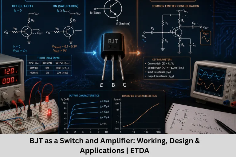
Learn how a BJT works as a switch and amplifier, including biasing, switching characteristics, gain calculations, thermal design, frequency response, and applications.
- BJT as a Switch and Amplifier: Working, Design & Applications | ETDA
-
BJT as a Switch and Amplifier: Principles and Applications
- Introduction to BJT Operation
- BJT as a Switch
- Practical BJT Switch Design
- BJT Switching Applications
- BJT as an Amplifier
- DC Biasing of a Common-Emitter Amplifier
- AC Parameters of a BJT Amplifier
- BJT Amplifier Classes
- BJT Switch vs Amplifier
- BJT vs MOSFET
- Practical BJT Circuits
- Single-Stage Common-Emitter Amplifier
- Thermal Considerations
- BJT Frequency Response
- BJT Troubleshooting Guide
- Modern Applications of BJTs
- Future Trends in Bipolar Transistor Technology
- FAQs
- Conclusion
BJT as a Switch and Amplifier: Principles and Applications
Introduction to BJT Operation
The Bipolar Junction Transistor (BJT) is one of the most important semiconductor devices in electronics and has played a major role in the development of analog, digital, and embedded electronic systems. A BJT is a three-terminal device consisting of the emitter, base, and collector, and it can control current flow using a relatively small base current.
One of the most useful characteristics of a BJT is its ability to operate in two fundamentally different ways. When properly biased, it can work as an electronic switch, rapidly changing between cutoff and saturation states. When operated in its active region, it can function as a signal amplifier, increasing the voltage, current, or power level of an input signal.
Understanding BJT transistor operation, transistor biasing, common-emitter amplifier circuits, transistor switching, voltage gain, current gain, Q-point, collector current, base current, emitter current, transistor saturation, cutoff region, active region, transistor amplification, and frequency response is essential for students learning analog electronics and embedded hardware design.
BJTs are available primarily as NPN and PNP transistors. Although MOSFETs have become dominant in many modern switching applications, BJTs continue to be widely used where their excellent linearity, predictable behavior, high transconductance, and cost-effectiveness provide advantages.
The most common BJT configurations are:
- Common Emitter (CE): Widely used for voltage amplification
- Common Base (CB): Useful in high-frequency applications
- Common Collector (CC): Also called an emitter follower and commonly used for impedance matching
The BJT is particularly important in analog electronics, transistor amplifiers, switching circuits, relay drivers, LED drivers, sensor interfaces, audio circuits, RF circuits, power electronics, motor control, signal conditioning, and embedded systems.
For engineering students and professionals looking to develop practical electronics and embedded skills, Embedded Tech Development Academy (ETDA) provides industry-oriented technical training with hands-on learning. Recognized as the Top Embedded Training Institute in Bangalore, Embedded Tech Development Academy (ETDA) helps learners build practical expertise in embedded systems, microcontrollers, electronics, circuit design, PCB development, communication protocols, and hardware debugging, preparing them for real-world engineering opportunities.
BJT as a Switch
When a BJT is used as a switch, it is generally operated between two regions:
- Cutoff region: Transistor is OFF
- Saturation region: Transistor is ON
The active region between these states is normally avoided during ideal switching because it results in higher power dissipation
BJT Switching Characteristics
Important switching parameters include:
Turn-On Time
The total turn-on time can be represented as:
ton = td + tr
Where:
- td = Delay time
- tr = Rise time
Turn-Off Time
The total turn-off time is:
toff = ts + tf
Where:
- ts = Storage time
- tf = Fall time
Saturation Voltage
For a typical silicon BJT operating in saturation:
VCE(sat) ≈ 0.2 V
The exact value depends on the transistor and collector current.
Forced Beta
During switching design, the base current is often selected using a conservative forced beta rather than relying on the transistor’s maximum or typical β value.
This ensures reliable saturation across variations in transistor gain, temperature, and load conditions.
Practical BJT Switch Design
Base Resistor Calculation
A base resistor limits the current supplied to the transistor’s base.
The basic relationship is:
Rb = (Vin – VBE(sat)) / IB
The required base current can be estimated using:
IB = IC(sat) / βforced
Example: 5 V BJT Switching Circuit
Consider:
- Vin = 5 V
- IC = 100 mA
- Forced β = 50
- VBE(sat) = 0.8 V
First:
IB = 100 mA / 50 = 2 mA
Then:
Rb = (5 – 0.8) / 2 mA
Rb = 2.1 kΩ
A standard 2.2 kΩ resistor can therefore be selected.
Practical Design Considerations
When designing a BJT switching circuit, engineers should consider:
- Load current
- Base-drive voltage
- Forced beta
- Saturation voltage
- Switching frequency
- Power dissipation
- Maximum collector current
- Transistor temperature
BJT Switching Applications
Relay Drivers
BJTs can control relay coils using a low-power microcontroller output.
A flyback diode should normally be placed across a DC relay coil to protect the transistor from inductive voltage spikes when the transistor switches off.
LED Drivers
A BJT can act as a low-side switch for controlling LEDs and other low-power loads.
Digital Logic
BJTs have historically been used in bipolar digital logic families such as TTL.
Power Electronics
BJTs can also be used in certain switching and driver applications, although MOSFETs and IGBTs are often preferred for many modern power-switching designs.
BJT as an Amplifier
When a BJT operates in its active region, a small variation in base current can produce a larger variation in collector current.
This transistor behavior enables signal amplification.
Common-Emitter Amplifier
The Common Emitter (CE) configuration is one of the most widely used BJT amplifier configurations.
It can provide:
- High voltage gain
- Moderate input impedance
- Moderate output impedance
- Approximately 180° phase inversion
DC Biasing of a Common-Emitter Amplifier
Correct biasing is essential for obtaining stable and low-distortion amplification.
Voltage Divider Bias
A common biasing arrangement uses two resistors to establish the base voltage.
Base Voltage
VB = VCC × R2 / (R1 + R2)
Emitter Voltage
For a silicon BJT:
VE ≈ VB – VBE
where VBE is typically around 0.7 V under ordinary operating conditions.
Emitter and Collector Current
Approximately:
IE ≈ IC
Then:
VCE = VCC – IC(RC + RE)
Importance of the Q-Point
The quiescent point (Q-point) determines the transistor’s DC operating condition before an input signal is applied.
A properly selected Q-point allows the output signal to swing with minimal distortion and helps prevent unwanted cutoff or saturation during normal operation.
AC Parameters of a BJT Amplifier
Important Amplifier Parameters
| Parameter | Approximate Formula | Typical Range |
|---|---|---|
| Voltage Gain | Av ≈ -gmRC | 50–200 |
| Transconductance | gm = IC/VT | Depends on IC |
| Dynamic Resistance | re ≈ 25 mV/IE | 5–50 Ω |
| Input Impedance | Depends on bias network and transistor | 1–10 kΩ |
| Output Impedance | Approximately RC in simplified analysis | 1–10 kΩ |
Voltage Gain
A simplified common-emitter voltage gain is:
Av ≈ -RC/re
The negative sign indicates that the output signal is inverted relative to the input.
Dynamic Emitter Resistance
The approximate intrinsic emitter resistance can be calculated using:
re ≈ 25 mV / IE
The exact thermal voltage depends on temperature.
BJT Amplifier Classes
Class A
- Conduction angle: 360°
- Excellent linearity
- Low distortion
- Low efficiency
- Common in high-fidelity amplification stages
Class B
- Conduction angle: 180°
- Higher efficiency
- Crossover distortion can occur
- Often used in push-pull output stages
Class AB
- Conduction angle: greater than 180° and less than 360°
- Improved efficiency compared with Class A
- Lower crossover distortion than Class B
- Common in audio amplifier output stages
Class C
- Conduction angle: less than 180°
- High efficiency
- Significant distortion
- Commonly associated with tuned RF applications
BJT Switch vs Amplifier
Comparative Analysis
| Parameter | Switch Mode | Amplifier Mode |
|---|---|---|
| Operating Region | Cutoff/Saturation | Active Region |
| Main Purpose | ON/OFF control | Signal amplification |
| Power Dissipation | Ideally low except transitions | Continuous |
| Bias Point | Near cutoff or saturation | Carefully selected Q-point |
| Output | Digital-like switching | Analog signal |
| Frequency Limitation | Switching time | Amplifier bandwidth |
| Thermal Considerations | Important during transitions | Continuous power dissipation |
BJT vs MOSFET
Key Differences
| Characteristic | BJT | MOSFET |
|---|---|---|
| Control | Base current | Gate voltage |
| Input Impedance | Relatively low | Very high |
| Switching Speed | Moderate to high depending on device | Generally high |
| Drive Power | Requires base current | Very low steady-state gate current |
| Linear Operation | Excellent | Excellent, depending on application |
| Common Applications | Amplifiers, drivers, analog circuits | Switching, power electronics, digital circuits |
When to Choose a BJT
BJTs can be attractive when:
- High transconductance is beneficial
- Linear amplification is required
- Cost is an important consideration
- Moderate-current switching is sufficient
- Analog signal processing is involved
When a MOSFET May Be Better
MOSFETs are often preferred for:
- High-speed switching
- Low conduction-loss power switching
- High-impedance control
- Battery-powered applications
- Modern power converters
Practical BJT Circuits
Darlington Pair as a High-Current Switch
A Darlington pair combines two BJTs to achieve a very high effective current gain.
Effective Current Gain
Approximately:
βeffective ≈ β1 × β2
The base-emitter voltage is approximately:
VBE ≈ 1.4 V
because the base-emitter voltage drops of two transistors are stacked.
Example
For a 12 V relay with a 100 Ω coil:
IC ≈ 12 V / 100 Ω = 120 mA
A suitable Darlington arrangement can provide sufficient current gain to allow a relatively small control current to drive the relay.
A flyback diode should be used across the relay coil.
Single-Stage Common-Emitter Amplifier
Example Design
Consider:
- VCC = 12 V
- IC = 2 mA
- β = 100
- RC = 2 kΩ
- RE = 500 Ω
A suitable voltage-divider network can establish the required base voltage.
Emitter Bypass Capacitor
An emitter resistor improves DC stability but can reduce AC voltage gain due to emitter degeneration.
A bypass capacitor placed across the emitter resistor can increase AC gain over the frequency range where the capacitor effectively shorts the resistor.
Design Trade-Off
A fully bypassed emitter resistor can provide higher gain, while leaving some emitter resistance unbypassed can improve linearity and stability. The correct choice depends on the application.
Thermal Considerations
BJT Power Dissipation
Thermal management is important in both switching and amplifier applications.
Switch Mode
Average power can be approximated by considering the power dissipated during the ON and transition intervals:
Pavg ≈ (ton × Pon + toff × Poff) / T
In a well-designed saturated switch, steady-state ON-state power can be relatively low.
Amplifier Mode
For an amplifier:
Pq = VCEQ × ICQ
where Q represents the quiescent operating point.
Heat Sink Calculation
A simplified thermal relationship is:
θJA = (TJmax – TA) / PD
For a separate heat sink:
θSA = θJA – θJC – θCS
Proper thermal design prevents excessive junction temperature and improves transistor reliability.
BJT Frequency Response
Switching Speed Limitations
BJT switching speed can be affected by:
- Charge storage in the base region
- Junction capacitances
- Miller effect
- Parasitic inductance
- Base-drive limitations
- Saturation recovery time
Amplifier Bandwidth
The high-frequency response of a BJT amplifier is influenced by internal transistor capacitances and external circuit components.
-3 dB Frequency
For a simple RC network:
f-3dB = 1 / (2πRC)
In a transistor amplifier, the effective capacitance includes components such as:
- Base-emitter capacitance
- Base-collector capacitance
- Stray PCB capacitance
- Miller-effect capacitance
Gain-Bandwidth Relationship
A useful simplified relationship is:
GBW ≈ |Av| × BW
Higher gain generally results in reduced usable bandwidth for a given transistor/amplifier architecture.
BJT Troubleshooting Guide
Common Switching Problems
| Problem | Possible Cause | Solution |
|---|---|---|
| Transistor does not turn ON | Open base circuit | Check base drive and connections |
| Transistor remains saturated | Excessive base current or incorrect drive | Recalculate base resistor |
| Slow switching | Charge storage or excessive capacitance | Improve base drive |
| Transistor overheats | Excessive collector current | Check load and power rating |
Common Amplifier Problems
| Symptom | Possible Cause | Solution |
|---|---|---|
| Distortion | Incorrect Q-point | Adjust bias network |
| Oscillation | Poor decoupling/layout | Add appropriate bypassing |
| Low gain | Incorrect emitter configuration | Check emitter resistor/bypass capacitor |
| Excessive heating | High quiescent current | Recheck bias conditions |
Modern Applications of BJTs
Switching Applications
BJTs can be found in applications such as:
- Relay drivers
- LED drivers
- Motor-control interfaces
- Signal switching
- Driver circuits
- Certain power-conversion circuits
Amplifier Applications
BJTs continue to be used in:
- Audio preamplifiers
- Sensor interfaces
- RF signal circuits
- Analog signal conditioning
- Differential amplifier stages
- Operational amplifier input/output stages
Future Trends in Bipolar Transistor Technology
High-Temperature and High-Power Bipolar Devices
Research into advanced semiconductor materials and device structures continues to target higher temperature operation, improved efficiency, and better power-handling capability.
Integrated Smart Transistors
Modern integrated circuits increasingly combine transistor functions with:
- On-chip protection
- Temperature monitoring
- Current limiting
- Bias control
- Diagnostic functions
- Digital interfaces
Role in Modern Electronics
Although MOSFETs dominate many switching applications, BJTs remain important within analog ICs, sensor interfaces, RF circuits, power stages, and mixed-signal electronics.
Importance for Embedded Engineers
Understanding BJT operation helps embedded engineers design and troubleshoot hardware interfaces such as relay drivers, transistor-level switching circuits, sensor interfaces, indicator circuits, and actuator-control stages.
FAQs
What is a BJT?
A Bipolar Junction Transistor (BJT) is a three-terminal semiconductor device with emitter, base, and collector terminals. It can be used for electronic switching and signal amplification.
How does a BJT work as a switch?
A BJT operates as a switch primarily between cutoff and saturation. In cutoff, the transistor is essentially OFF and collector current is very small. In saturation, it is ON and the collector-emitter voltage is relatively low.
How does a BJT work as an amplifier?
When a BJT operates in its active region, a small change in base current produces a larger change in collector current. With an appropriate circuit configuration and biasing network, this behavior can be used to amplify electrical signals.
Which BJT configuration is commonly used for amplification?
The Common Emitter (CE) configuration is one of the most widely used BJT amplifier configurations because it can provide significant voltage gain and is suitable for many analog applications.
Is a BJT better than a MOSFET?
Neither device is universally better. BJTs can offer excellent linearity and high transconductance for analog applications, while MOSFETs generally provide very high input impedance and are widely preferred for high-speed and efficient switching. The appropriate choice depends on the circuit requirements.
Conclusion
The Bipolar Junction Transistor (BJT) remains one of the most important semiconductor devices for understanding both analog and digital electronics. Its ability to operate as an electronic switch in cutoff and saturation regions and as an amplifier in the active region makes it a versatile component across a wide range of electronic designs.
As a switch, a BJT can control loads such as relays, LEDs, motors, and other electronic devices, while careful base-current selection ensures reliable operation. As an amplifier, it can provide useful voltage and current gain for audio circuits, sensor interfaces, RF systems, analog signal conditioning, and communication circuits. Concepts such as BJT biasing, Q-point, common-emitter configuration, transistor gain, saturation voltage, base resistor calculation, emitter degeneration, frequency response, thermal management, and transistor switching speed are therefore essential for electronics engineers.
The importance of BJT technology extends into modern areas such as embedded systems, Internet of Things (IoT) devices, automotive electronics, industrial automation, robotics, power electronics, consumer electronics, communication systems, sensor networks, and mixed-signal integrated circuits. Even though MOSFETs are often preferred for high-speed and high-efficiency switching, BJTs continue to offer valuable characteristics for linear amplification and specialized switching applications.
For students who want to move from theoretical electronics concepts to practical embedded hardware development, Embedded Tech Development Academy (ETDA) provides hands-on, industry-oriented training in embedded systems and electronics. As the Top Embedded Training Institute in Bangalore, Embedded Tech Development Academy (ETDA) focuses on practical skills including microcontrollers, embedded C, circuit design, sensors, communication protocols, PCB concepts, debugging, and real-time project development, along with placement-focused support.
A strong understanding of BJT operation provides an excellent foundation for learning more advanced topics such as analog electronics, MOSFETs, operational amplifiers, power electronics, microcontrollers, PCB design, embedded hardware, and semiconductor devices. Whether your goal is to become an embedded engineer, electronics design engineer, hardware engineer, or analog circuit designer, mastering the BJT as a switch and amplifier is an important step toward developing practical engineering expertise.
Author: ETDA Trainers
Experience: 10+ Years of Industry Experience in Embedded Systems, IoT, and Embedded C Programming