
Design and Verification of Digital Circuits: Complete Guide to RTL, UVM & Verification
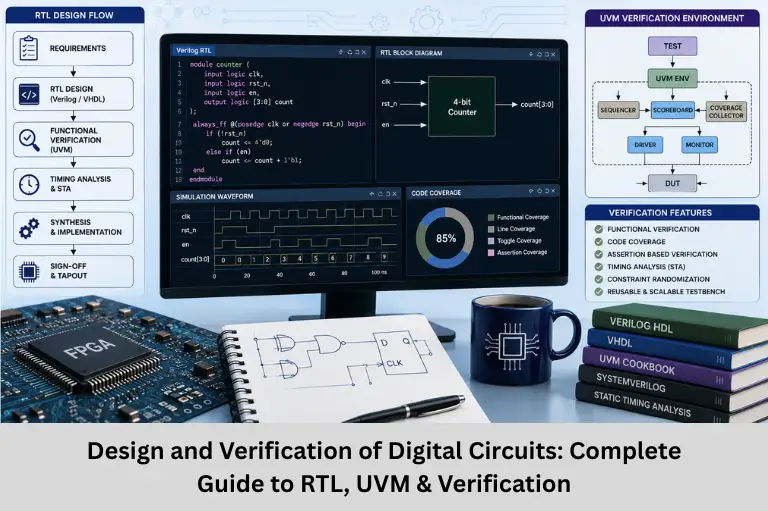
Learn digital circuit design and verification, including RTL design, Verilog, VHDL, UVM, STA, functional verification, timing analysis, and modern semiconductor verification techniques.
- Design and Verification of Digital Circuits: Complete Guide to RTL, UVM & Verification
-
Introduction to Digital Circuit Design and Verification
- Digital Circuit Design Flow
- Hardware Description Languages (HDLs)
- Modern Verification Methodologies
- Functional Verification Techniques
- Timing Analysis and Design Constraints
- Power-Aware Design Verification
- Emerging Verification Technologies
- Industry-Standard Design and Verification Tools
- Real-World Verification Case Studies
- Future Trends in Digital Circuit Verification
- Career Opportunities in Digital Design and Verification
- Frequently Asked Questions (FAQs)
- Conclusion
Introduction to Digital Circuit Design and Verification
Digital circuit design and verification are the backbone of the semiconductor industry, enabling the development of reliable, high-performance integrated circuits used in smartphones, computers, automotive electronics, medical devices, networking equipment, aerospace systems, and artificial intelligence hardware. As semiconductor technology advances toward smaller process nodes and increasingly complex System-on-Chip (SoC) architectures, ensuring the correctness and reliability of digital circuits before fabrication has become more important than ever.
Modern chip development follows a structured design flow that transforms a concept into silicon. Engineers begin by defining functional specifications, creating RTL (Register Transfer Level) designs using Hardware Description Languages (HDLs), verifying functionality through simulation and formal methods, synthesizing the design into logic gates, performing physical implementation, and finally validating the fabricated silicon. Verification now accounts for nearly 60–70% of the overall chip development effort, making it one of the most critical phases in VLSI design.
Understanding concepts such as Digital Logic Design, RTL Design, Verilog, VHDL, SystemVerilog, Universal Verification Methodology (UVM), Functional Verification, Assertion-Based Verification (ABV), Static Timing Analysis (STA), Clock Domain Crossing (CDC), FPGA Prototyping, ASIC Design Flow, Design for Testability (DFT), Formal Verification, Coverage Analysis, Logic Synthesis, Physical Design, Place and Route (PnR), Low Power Design, SoC Verification, Semiconductor Testing, and Silicon Validation is essential for aspiring VLSI and semiconductor engineers.
With the rapid growth of Artificial Intelligence (AI), Machine Learning (ML), 5G communication, automotive electronics, Internet of Things (IoT) devices, edge computing, high-performance processors, cloud infrastructure, and advanced semiconductor technologies, the demand for engineers skilled in digital design and verification continues to rise worldwide.
To help students build industry-ready skills, Embedded Tech Development Academy (ETDA) offers practical, placement-oriented training in Digital Electronics, VLSI Design, Verilog, SystemVerilog, UVM, FPGA, Embedded Systems, Embedded C, ARM Cortex, PCB Design, Internet of Things (IoT), and Semiconductor Technologies. Through hands-on laboratory sessions, industry projects, and expert mentorship, Embedded Tech Development Academy (ETDA) prepares aspiring engineers for rewarding careers in semiconductor design, chip verification, and embedded systems development.
This comprehensive guide explores the complete digital circuit design flow, verification methodologies, HDL programming, timing analysis, power-aware verification, industry-standard tools, real-world applications, and emerging trends shaping modern semiconductor engineering.
Digital Circuit Design Flow
A successful digital chip follows a systematic design methodology.
Key Design Stages
1. Specification
The process begins with defining:
- Functional requirements
- Performance targets
- Power consumption goals
- Area constraints
- Cost objectives
2. Architecture Design
Engineers define:
- Functional blocks
- Data paths
- Interfaces
- Memory architecture
- Processing units
3. RTL Design
The architecture is implemented using Hardware Description Languages such as:
- Verilog
- VHDL
- SystemVerilog
4. Functional Verification
Verification ensures that the RTL behaves exactly as specified before fabrication.
5. Logic Synthesis
RTL is translated into a gate-level netlist using synthesis tools.
6. Physical Design
Physical implementation includes:
- Floorplanning
- Placement
- Clock Tree Synthesis
- Routing
- GDSII generation
7. Post-Silicon Validation
Fabricated chips undergo extensive laboratory testing before mass production.
Importance of the Design Flow
A structured design flow minimizes costly silicon re-spins and accelerates product development.
Hardware Description Languages (HDLs)
Hardware Description Languages describe digital hardware behavior and structure.
Verilog vs VHDL
| Feature | Verilog | VHDL |
|---|---|---|
| Syntax | C-like | ADA-like |
| Learning Curve | Easier | More Structured |
| Strong Typing | No | Yes |
| Popularity | USA & Asia | Europe |
| Verification Support | SystemVerilog | OSVVM |
Choosing an HDL
Verilog and SystemVerilog are widely adopted in ASIC and FPGA development due to their simplicity and extensive industry support.
Modern Verification Methodologies
Verification ensures functional correctness before manufacturing.
Verification Spectrum
Modern verification includes:
- Simulation
- FPGA Emulation
- Formal Verification
- Hardware Validation
Universal Verification Methodology (UVM)
UVM has become the industry standard for functional verification.
UVM Testbench Components
- Test
- Sequence
- Driver
- Interface
- Device Under Test (DUT)
- Monitor
- Scoreboard
- Functional Coverage
- Assertions
UVM Phases
- Build Phase
- Connect Phase
- Run Phase
- Report Phase
Why UVM?
UVM promotes reusable verification components, scalable testbenches, and standardized verification across complex System-on-Chip (SoC) projects.
Functional Verification Techniques
Functional verification ensures that all intended design behaviors are tested.
Assertion-Based Verification (ABV)
Assertions automatically check design behavior during simulation.
Benefits include:
- Early bug detection
- Improved debugging
- Reduced verification time
Coverage Metrics
| Coverage Type | Purpose |
|---|---|
| Code Coverage | Line and branch execution |
| Functional Coverage | Scenario verification |
| Toggle Coverage | Signal transition analysis |
| FSM Coverage | State transition verification |
AI accelerators enable faster machine learning and neural network processing.
Timing Analysis and Design Constraints
Meeting timing requirements is essential for reliable chip operation.
Static Timing Analysis (STA)
STA verifies timing without applying input vectors.
Engineers analyze:
- Setup Time
- Hold Time
- Clock Skew
- Clock Latency
- Critical Paths
Timing Constraints
Common constraints include:
- Clock definitions
- Input delay
- Output delay
- False paths
- Multi-cycle paths
Why STA Matters
Static Timing Analysis prevents timing violations that could cause functional failures in silicon.
Power-Aware Design Verification
Modern chips must balance performance with energy efficiency.
Power Estimation Methods
Methods include:
- Static Power Analysis
- Dynamic Power Analysis
- Post-Silicon Measurements
Low-Power Verification
Verification checks include:
- Clock Gating
- Isolation Cells
- Retention Registers
- Power Domain Crossing
Emerging Verification Technologies
Semiconductor verification is evolving rapidly.
Artificial Intelligence in Verification
AI assists engineers by:
- Predicting bugs
- Automating test generation
- Identifying coverage gaps
- Optimizing verification plans
Formal Verification
Formal verification mathematically proves circuit correctness.
Applications include:
- Property Checking
- Equivalence Checking
- Security Verification
Industry-Standard Design and Verification Tools
Professional semiconductor companies use advanced EDA tools.
Design Tools
Examples include:
- Cadence Genus
- Synopsys Design Compiler
- Siemens EDA
Verification Tools
Popular verification tools include:
- Synopsys VCS
- Cadence Xcelium
- Siemens Questa
- Synopsys ZeBu
Importance of EDA Tools
Electronic Design Automation (EDA) software accelerates chip development while improving design quality and verification efficiency.
Real-World Verification Case Studies
CPU Pipeline Verification
Verification challenges include:
- Data Hazards
- Control Hazards
- Pipeline Stalls
- Branch Prediction
- Speculative Execution
Solutions include:
- Directed Tests
- Randomized Testing
- Compliance Verification
SerDes PHY Validation
Validation techniques include:
- Eye Diagram Analysis
- Jitter Testing
- Mixed-Signal Simulation
- High-Speed Signal Integrity Analysis
Future Trends in Digital Circuit Verification
The semiconductor industry continues adopting advanced verification techniques.
Shift-Left Verification
Benefits include:
- Earlier bug detection
- Reduced development cost
- Faster product release
Quantum Circuit Verification
Future verification will include:
- Quantum Logic Verification
- Qubit Modeling
- Quantum Error Correction
AI-Driven Verification Automation
Future tools will increasingly automate:
- Test generation
- Bug localization
- Coverage closure
- Verification planning
Future Outlook
AI-powered verification, formal methods, and automation will significantly improve first-pass silicon success rates.
Career Opportunities in Digital Design and Verification
Professionals with verification expertise can pursue careers such as:
- RTL Design Engineer
- Verification Engineer
- FPGA Engineer
- ASIC Design Engineer
- Physical Design Engineer
- DFT Engineer
- STA Engineer
- SoC Verification Engineer
- Semiconductor Validation Engineer
- VLSI Design Engineer
Frequently Asked Questions (FAQs)
What is digital circuit verification?
Digital circuit verification is the process of ensuring that a digital design functions according to its specifications before semiconductor fabrication using simulation, formal verification, emulation, and hardware testing.
Why is UVM widely used in chip verification?
Universal Verification Methodology (UVM) provides reusable, scalable, and standardized verification environments that improve productivity and simplify the verification of complex ASIC and SoC designs.
What is the difference between Verilog and VHDL?
Verilog has a C-like syntax and is generally easier to learn, while VHDL is strongly typed with an ADA-like syntax, making it more structured for complex hardware designs.
What is Static Timing Analysis (STA)?
Static Timing Analysis (STA) is a verification technique that checks setup time, hold time, clock skew, and critical timing paths without requiring simulation vectors, ensuring reliable chip timing performance.
What career opportunities are available in digital design and verification?
Professionals can work as RTL Design Engineers, Verification Engineers, FPGA Engineers, ASIC Engineers, SoC Verification Engineers, Physical Design Engineers, DFT Engineers, STA Engineers, Semiconductor Validation Engineers, and VLSI Design Engineers in leading semiconductor and electronics companies.
Conclusion
Digital circuit design and verification are essential pillars of the modern semiconductor industry. From RTL design, Verilog, VHDL, SystemVerilog, UVM, Functional Verification, Assertion-Based Verification, Static Timing Analysis (STA), Logic Synthesis, FPGA Design, ASIC Development, Design for Testability (DFT), Physical Design, Place and Route (PnR), Clock Domain Crossing (CDC), Power-Aware Verification, SoC Verification, Silicon Validation, Semiconductor Testing, Electronic Design Automation (EDA), Artificial Intelligence (AI), and Machine Learning (ML) to advanced chip manufacturing, every stage contributes to delivering reliable, high-performance integrated circuits.
As semiconductor technologies continue advancing with AI processors, autonomous vehicles, 5G communication, cloud computing, edge AI, Internet of Things (IoT), quantum computing, and next-generation SoC architectures, the demand for highly skilled digital design and verification engineers is growing rapidly across the global semiconductor ecosystem.
Embedded Tech Development Academy (ETDA) equips aspiring engineers with practical, industry-focused training in Digital Electronics, VLSI Design, Verilog, SystemVerilog, FPGA Development, UVM, Embedded Systems, Embedded C, ARM Cortex, PCB Design, Internet of Things (IoT), and Semiconductor Technologies. Through hands-on projects, expert-led instruction, and placement-oriented programs, Embedded Tech Development Academy (ETDA) helps students build strong technical foundations and prepares them for successful careers in ASIC design, semiconductor verification, embedded engineering, and advanced chip development.
Whether you are an engineering student, electronics enthusiast, or working professional, mastering digital circuit design and verification opens exciting opportunities in one of the world’s fastest-growing and most innovative technology industries.
Author: ETDA Trainers
Experience: 10+ Years of Industry Experience in Embedded Systems, IoT, and Embedded C Programming