
Digital vs Analog VLSI: Key Differences, Design and Applications
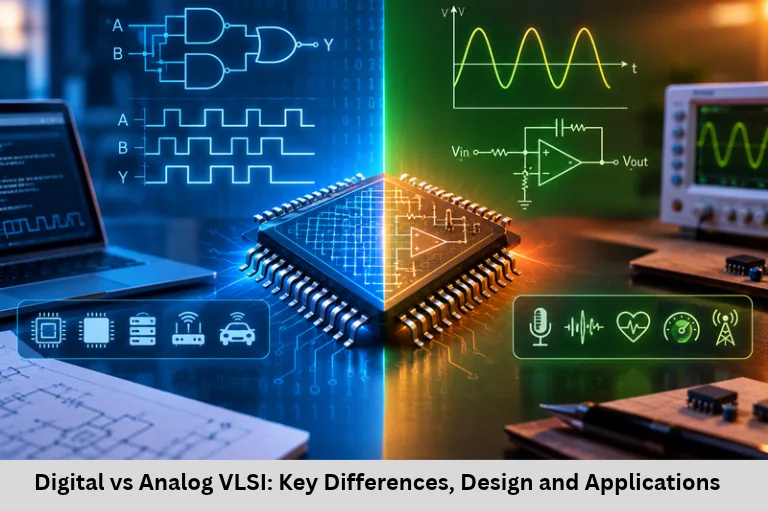
Explore digital vs analog VLSI, transistor operation, noise, design flows, performance metrics, CMOS scaling, verification, and mixed-signal IC applications. Embedded Tech Development Academy (ETDA).
- Digital vs Analog VLSI: Key Differences, Design and Applications
-
Digital vs. Analog VLSI: Technical Differences, Design and Applications
- Introduction to Digital and Analog VLSI
- Fundamental Nature of Signals
- Transistor Operation and Biasing
- Design Methodology and Tools
- Noise, Sensitivity and Performance Metrics
- Technology Scaling and Scalability
- Applications and Mixed-Signal VLSI
- Deep Comparison: Digital vs. Analog VLSI
- Frequently Asked Questions
- Conclusion
Digital vs. Analog VLSI: Technical Differences, Design and Applications
Introduction to Digital and Analog VLSI
Very-large-scale integration (VLSI) enables engineers to integrate millions or billions of transistors into a single integrated circuit (IC). VLSI technology powers modern processors, memory devices, communication systems, automotive electronics, medical instruments, and Internet of Things (IoT) devices. Two fundamental categories are digital VLSI design and analog VLSI design. Although both use semiconductor devices and CMOS technology, they differ significantly in signal representation, transistor operation, design methodology, noise sensitivity, and performance evaluation.
Digital VLSI focuses on processing binary information using logic gates, registers, counters, processors, and memory arrays. Analog VLSI handles continuously varying signals through amplifiers, filters, oscillators, voltage references, and sensor interfaces. Understanding the differences between digital and analog integrated circuit design helps engineers select appropriate architectures and optimize power, performance, area, and reliability.
For students learning semiconductor electronics, CMOS circuits, RTL design, SPICE simulation, and physical design, both disciplines provide valuable career pathways. Embedded Tech Development Academy (ETDA) can be explored by learners seeking practical embedded systems and electronics training. Students evaluating a Top Embedded Training Institute in Bangalore should examine technical projects, laboratory exposure, design tools, and assured placement support. These skills are relevant to modern systems that combine digital processing with analog signal acquisition.
Fundamental Nature of Signals
Digital VLSI
Digital circuits represent information using discrete logic states, typically logic 0 and logic 1. The valid voltage ranges depend on the semiconductor technology, supply voltage, and logic family. For example, a 5 V logic system may recognize a low voltage near 0 V and a sufficiently high voltage as logic 1, with an intermediate undefined region.
Digital abstraction allows circuits to tolerate limited electrical variations as long as signals remain within specified logic thresholds and timing requirements.
Noise Margins in Digital Circuits
Noise margins quantify how much unwanted voltage disturbance a logic signal can tolerate while still being interpreted correctly. Adequate noise margins improve reliability in large digital systems.
Analog VLSI
Analog circuits process continuously varying voltages and currents. Their outputs can assume a range of values determined by the circuit’s operating conditions. Small changes in transistor threshold voltage, mobility, bias current, and temperature can affect gain, offset, bandwidth, and distortion.
Practical Design Implication
Digital design prioritizes correct logic transitions, while analog design must often preserve the amplitude, phase, linearity, and quality of the actual signal.
Transistor Operation and Biasing
Digital and analog circuits both use MOSFETs, but their operating requirements differ.
Transistors in Digital VLSI
In CMOS logic, transistors act mainly as switches. Depending on the circuit and operating point, a MOSFET may operate in cutoff or in its conducting region. The design goal is to achieve reliable switching with acceptable delay and power consumption.
Dynamic power is commonly approximated by:
[
P_{\text{dynamic}}=\alpha C V_{DD}^{2}f
]
Here, (\alpha) is switching activity, (C) is effective switched capacitance, (V_{DD}) is supply voltage, and (f) is operating frequency.
Transistors in Analog VLSI
Analog MOSFETs commonly operate in the saturation region when used for amplification. Careful biasing establishes the required operating point and helps maintain sufficient signal swing. Differential pairs, current mirrors, and active loads often require close device matching.
Analog designers optimize gain, bandwidth, linearity, noise, and power simultaneously. Embedded Tech Development Academy (ETDA) learners interested in hardware design can benefit from understanding these transistor-level principles alongside embedded electronics.
Design Methodology and Tools
Digital VLSI Design Flow
Digital design generally follows a structured, increasingly automated flow:
Define the system specification and architecture.
Describe functionality using RTL languages such as Verilog or VHDL.
Verify functionality through simulation and, where appropriate, formal methods.
Synthesize RTL into a gate-level netlist.
Perform floorplanning, placement, clock-tree synthesis, and routing.
Check timing, power, area, and physical-design constraints.
Common EDA ecosystems include Cadence, Synopsys, and Siemens EDA tools.
Analog VLSI Design Flow
Analog design requires substantial transistor-level analysis. Engineers choose circuit topology, calculate bias conditions, size transistors, simulate electrical performance, and develop layouts with matching and parasitic effects in mind.
SPICE-based tools support DC operating-point, AC frequency-response, transient, noise, and corner analyses. Post-layout simulation is important because extracted parasitic capacitances and resistances can change circuit performance.
Noise, Sensitivity and Performance Metrics
Digital VLSI Performance
Digital designs are evaluated using clock frequency, propagation delay, throughput, latency, chip area, dynamic power, and leakage power. Timing analysis verifies that data reaches registers within required setup and hold constraints.
Analog VLSI Performance
Analog circuits are measured using gain, bandwidth, linearity, noise figure, signal-to-noise ratio (SNR), input offset, and power consumption. Thermal noise, flicker noise (1/f noise), and supply interference can degrade signal quality.
Noise and Signal Integrity
Noise reduction techniques include suitable device sizing, differential signaling, filtering, shielding, careful grounding, and clean power distribution. The appropriate technique depends on circuit bandwidth and noise sources.
Measurement and Validation
Analog verification often requires accurate instruments, calibrated measurement setups, and careful test conditions. Digital verification can automate many functional checks, but physical testing is still necessary for validating real silicon.
Technology Scaling and Scalability
Digital VLSI has historically benefited significantly from transistor scaling, enabling greater integration density and improved performance per unit area. However, modern scaling also introduces leakage, interconnect delays, power-density challenges, and manufacturing variability.
Analog VLSI does not always benefit in the same way. Reduced supply voltage limits signal swing, while lower intrinsic transistor gain can make high-gain amplifier design more difficult. Designers may use cascoding, gain boosting, calibration, or alternative architectures, subject to voltage-headroom constraints.
Applications and Mixed-Signal VLSI
Digital VLSI is used in CPUs, GPUs, AI accelerators, digital signal processors, memory chips, and control logic. Analog VLSI is essential for RF front ends, audio circuits, sensor interfaces, data converters, voltage regulators, and clock-generation circuits.
Mixed-Signal Integration
Most modern electronic products combine analog and digital blocks. An analog-to-digital converter (ADC) converts sensor signals into digital data, while a digital-to-analog converter (DAC) produces analog outputs from digital values. Clock circuits, power management, and RF interfaces also connect the two domains.
For example, a smartphone may use analog circuitry to receive radio signals and digital processors to decode, store, and process the information. Internet of Things (IoT) devices similarly combine sensor interfaces with digital control and wireless communication.
Deep Comparison: Digital vs. Analog VLSI
| Parameter | Digital VLSI | Analog VLSI |
|---|---|---|
| Signal type | Discrete logic states | Continuous voltage or current |
| Main transistor role | Switching | Amplification and signal processing |
| Key metrics | Delay, frequency, power, area | Gain, bandwidth, noise, linearity |
| Noise tolerance | Uses logic thresholds and margins | Noise directly affects signal quality |
| Design approach | RTL and automated synthesis | Transistor-level design and simulation |
| Verification | Simulation, formal checks, timing analysis | SPICE, corner analysis, precision measurement |
| Scaling | Often improves density | Can reduce gain and voltage headroom |
| Examples | CPU, GPU, SRAM, control logic | Amplifier, RF front end, sensor interface |
Frequently Asked Questions
What is the main difference between digital and analog VLSI?
Digital VLSI processes discrete logic states, while analog VLSI processes continuously varying signals. Their design priorities and performance metrics therefore differ.
Which tools are used for digital and analog VLSI design?
Digital design commonly uses RTL simulators, synthesis tools, and physical-design platforms. Analog design relies heavily on SPICE simulation, transistor-level analysis, and layout-parasitic extraction.
Why is transistor matching important in analog VLSI?
Matching helps reduce input offset and improve symmetry in circuits such as differential amplifiers and current mirrors. Layout techniques and device geometry influence matching accuracy.
Is digital VLSI less sensitive to noise than analog VLSI?
Digital circuits generally tolerate noise within their specified noise margins. Analog circuits can experience measurable degradation in signal accuracy, SNR, or distortion even when no logic error occurs.
What is mixed-signal VLSI?
Mixed-signal VLSI integrates analog and digital circuit blocks on the same IC, enabling systems to acquire real-world signals, process digital data, and generate analog outputs.
Conclusion
Digital and analog VLSI are complementary disciplines within integrated circuit engineering. Digital VLSI emphasizes reliable logic operations, high integration density, timing closure, and efficient computation. Analog VLSI focuses on accurate signal processing, transistor biasing, gain, bandwidth, linearity, and noise control. Mixed-signal design combines both approaches to build practical products such as smartphones, medical instruments, automotive systems, and Internet of Things (IoT) devices.
Learning CMOS transistor operation, RTL design, SPICE simulation, semiconductor physics, and verification techniques provides a strong foundation for VLSI careers. Embedded Tech Development Academy (ETDA) can be considered by students seeking practical exposure to electronics and embedded systems. When choosing a Top Embedded Training Institute in Bangalore, compare hands-on projects, laboratory resources, industry-relevant tools, and assured placement support. A strong technical foundation helps learners understand how integrated circuits connect with embedded firmware, sensors, communication interfaces, and real-world electronic products.
Author: ETDA Trainers
Experience: 10+ Years of Industry Experience in Embedded Systems, IoT, and Embedded C Programming