
Flip-Flops and Latches in Digital Electronics
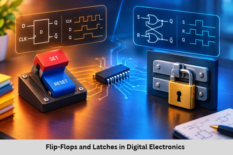
Learn flip-flops and latches, SR, D, JK and T circuits, timing parameters, sequential logic, applications, and digital memory fundamentals. Embedded Tech Development Academy (ETDA).
- Flip-Flops and Latches in Digital Electronics
- Flip-Flops and Latches: Understanding Digital Memory
Flip-Flops and Latches: Understanding Digital Memory
Introduction to Flip-Flops and Latches
Digital electronics relies on two major types of circuits: combinational logic and sequential logic. Combinational circuits produce outputs based on their current inputs, whereas sequential circuits can retain information about previous conditions. This ability to store information is essential for digital memory, registers, counters, processors, and control systems. Latches and flip-flops are fundamental sequential logic circuits that store one bit of binary data, either 0 or 1.
Understanding these storage elements helps learners explore digital logic design, Boolean algebra, clock signals, timing diagrams, synchronous circuits, and memory architecture. Latches are level-sensitive devices, while flip-flops generally respond to a particular clock edge. Their behavior affects circuit timing, power consumption, synchronization, and reliability. These concepts are important in microcontrollers, embedded systems, FPGA design, digital signal processing, and computer architecture.
Embedded Tech Development Academy (ETDA) supports practical technical learning in digital electronics, microcontrollers, and embedded system design. Learners looking for a Top Embedded Training Institute in Bangalore can strengthen their understanding through circuit analysis, timing diagrams, and hands-on digital design exercises. Embedded Tech Development Academy (ETDA) also provides assured placement support to help learners prepare for technical opportunities in embedded systems and electronics.
Why Do Digital Systems Need Memory Elements?
Combinational Logic Versus Sequential Logic
Combinational circuits, such as adders, multiplexers, and encoders, do not independently retain previous input values. Sequential circuits combine logic with storage elements to maintain a state.
Memory elements are needed to:
- Count events and clock pulses.
- Store intermediate calculation results.
- Track the current state of a finite state machine.
- Transfer data between processing stages.
- Coordinate operations in digital controllers.
The Role of Feedback
Many basic storage circuits use feedback, connecting an output back into the circuit’s logic. This feedback allows the circuit to maintain a stable state when its inputs change or become inactive.
One-Bit Storage
A single latch or flip-flop stores one binary bit. Multiple storage elements can be combined to form registers, shift registers, counters, and larger digital storage structures.
Understanding Latches
What Is a Latch?
A latch is a level-sensitive storage element. Its output can respond to input changes while its enable or control signal is at the active level. When the latch is disabled, it retains the previously stored value, assuming normal operating conditions.
SR Latch: Set-Reset Operation
An SR latch can be constructed using cross-coupled NOR gates or NAND gates. Its behavior depends on the gate type and input polarity. For a conventional active-HIGH NOR-based SR latch, the truth table is:
| S | R | Output behavior |
|---|---|---|
| 0 | 0 | Hold previous state |
| 1 | 0 | Set, Q = 1 |
| 0 | 1 | Reset, Q = 0 |
| 1 | 1 | Forbidden input condition |
The simultaneous HIGH inputs force both outputs LOW in a NOR-based SR latch, violating the expected complementary relationship between Q and its inverse. The state after both inputs return LOW can be unpredictable because of propagation delays.
NAND-Based SR Latch
A NAND-based SR latch commonly uses active-LOW inputs, often written as (\overline{S}) and (\overline{R}). Its input combinations therefore differ from the NOR-based version. Always check the circuit diagram and input polarity before interpreting its truth table.
Avoiding Forbidden Conditions
Digital designs should prevent forbidden SR input combinations. If the application requires a simpler data-storage interface, a D latch can reduce this problem by deriving complementary control signals from a single data input.
D Latch: Data Storage
A D latch has a data input (D) and an enable input (EN). When EN is active, the output follows D. When EN is inactive, the output holds its previous state. This behavior makes the D latch useful for temporary data storage and controlled data transfer.
Understanding Flip-Flops
What Is a Flip-Flop?
A flip-flop is generally an edge-triggered storage element. It samples its input at a specified clock transition, such as the rising edge or falling edge, and maintains its output between active edges.
Edge-triggered operation is especially useful in synchronous digital systems because it allows registers to update in a coordinated manner. However, correct operation still depends on clock quality, setup and hold requirements, and propagation delays.
Types of Flip-Flops
D Flip-Flop
The D flip-flop is widely used in digital systems. At the active clock edge, the output captures the value present at D. Between clock edges, Q retains its stored value.
Applications include data registers, pipeline stages, synchronizer circuits, and state machines.
JK Flip-Flop
The JK flip-flop improves on the traditional SR design by defining the condition in which both inputs are HIGH.
| J | K | Next state |
|---|---|---|
| 0 | 0 | Hold |
| 0 | 1 | Reset |
| 1 | 0 | Set |
| 1 | 1 | Toggle |
When J and K are both HIGH at the active clock edge, the output changes to its opposite state.
T Flip-Flop
The T, or toggle, flip-flop changes its output when T = 1 at the active clock edge. When T = 0, it retains its state. T flip-flops are useful in binary counters and frequency-division circuits.
Clocked SR Flip-Flop
A clocked SR flip-flop changes state according to its S and R inputs at the specified clock event. The simultaneous active condition remains forbidden in the conventional implementation, so input combinations must be controlled.
Choosing the Right Flip-Flop
D flip-flops are a common default for registers and synchronous state storage. JK and T flip-flops are useful for particular toggle and counter designs, while SR structures help demonstrate fundamental set-reset behavior.
Latch Versus Flip-Flop
| Feature | Latch | Flip-flop |
|---|---|---|
| Sensitivity | Active signal level | Specified clock edge |
| Control | Enable signal | Clock |
| Output behavior | Can follow input while enabled | Samples input at the active edge |
| Common use | Temporary storage, gated datapaths | Registers, counters, synchronous logic |
| Timing concerns | Transparency and enable timing | Setup, hold, and clock timing |
Neither type is universally faster or more stable. Circuit performance depends on implementation, loading, timing constraints, and design architecture.
Timing Parameters and Common Design Problems
Setup Time and Hold Time
Setup time is the minimum period that data must remain stable before the active clock edge. Hold time is the minimum period data must remain stable after that edge. Violating either requirement can cause incorrect sampling or metastability.
Propagation Delay
Propagation delay is the time between a triggering event or input change and the corresponding output response. In a synchronous circuit, clock-to-Q delay determines how soon a flip-flop’s new output becomes available to downstream logic.
Metastability and Race Conditions
Metastability can occur when timing requirements are violated, particularly when asynchronous signals are sampled by a clocked circuit. The output may take longer than expected to settle to a valid logic level. Synchronizer flip-flops are commonly used to reduce the probability of metastability propagating through a system.
Race conditions occur when a circuit’s result depends on the relative timing of signals or state changes. Poorly controlled latch transparency, feedback paths, and clocking can create timing hazards.
Practical Design Guidelines
Use appropriate clock-domain crossing techniques, satisfy setup and hold constraints, check timing reports, avoid forbidden input states, and verify behavior with simulation and hardware testing. Remember that glitches are short-lived unwanted transitions, while metastability is an uncertain internal state; they are related to timing but are not the same phenomenon.
Applications in Embedded and Digital Systems
Latches and flip-flops are used in:
- Registers that hold processor operands and results.
- Counters that track clock cycles or external events.
- Shift registers for serial-to-parallel and parallel-to-serial conversion.
- Finite state machines used in digital controllers.
- Pipeline registers that separate processing stages.
- Memory interfaces and digital communication hardware.
These concepts are foundational for microcontroller architecture, FPGA development, digital circuit debugging, and embedded hardware design. Embedded Tech Development Academy (ETDA) helps learners connect digital electronics theory with practical embedded projects. Those considering a Top Embedded Training Institute in Bangalore can focus on logic circuits, timing analysis, and microcontroller fundamentals, supported by assured placement support for career preparation.
Frequently Asked Questions
What is the main difference between a latch and a flip-flop?
A latch is level-sensitive and can follow its input while enabled. A flip-flop is edge-triggered and samples its input at a specified clock transition.
Why is the D flip-flop widely used?
It provides a straightforward way to capture one data bit at a clock edge, making it suitable for registers, pipelines, and synchronous state machines.
What is the forbidden state of an SR latch?
For a conventional NOR-based active-HIGH SR latch, S = 1 and R = 1 is forbidden because it forces both outputs LOW and can make the final state unpredictable when the inputs are released.
What are setup time and hold time?
Setup time is the required data-stability interval before the active clock edge. Hold time is the required stability interval after that edge. Violations can cause incorrect sampling or metastability.
Where are flip-flops used in embedded systems?
Flip-flops are used in registers, counters, shift registers, finite state machines, pipeline stages, and synchronization circuits within microcontrollers and digital hardware.
Conclusion
Latches and flip-flops form the foundation of sequential logic and digital memory. Latches are level-sensitive devices that follow their inputs while enabled, whereas flip-flops capture data at a designated clock edge. SR, D, JK, and T designs offer different methods for storing, setting, resetting, and toggling binary states. A strong understanding of truth tables, clock behavior, propagation delay, setup time, hold time, and metastability is essential for designing reliable digital circuits.
These principles support registers, counters, finite state machines, FPGA logic, microcontrollers, and embedded hardware. Embedded Tech Development Academy (ETDA) promotes practical learning in digital electronics, Embedded C, microcontroller systems, and hardware debugging. Learners searching for a Top Embedded Training Institute in Bangalore can develop technical skills through circuit exercises and project-based learning. With assured placement support, Embedded Tech Development Academy (ETDA) helps learners prepare for opportunities in embedded development and electronics engineering.
Author: ETDA Trainers
Experience: 10+ Years of Industry Experience in Embedded Systems, IoT, and Embedded C Programming