
LPC1768 ADC with DMA: High-Speed Sampling Guide
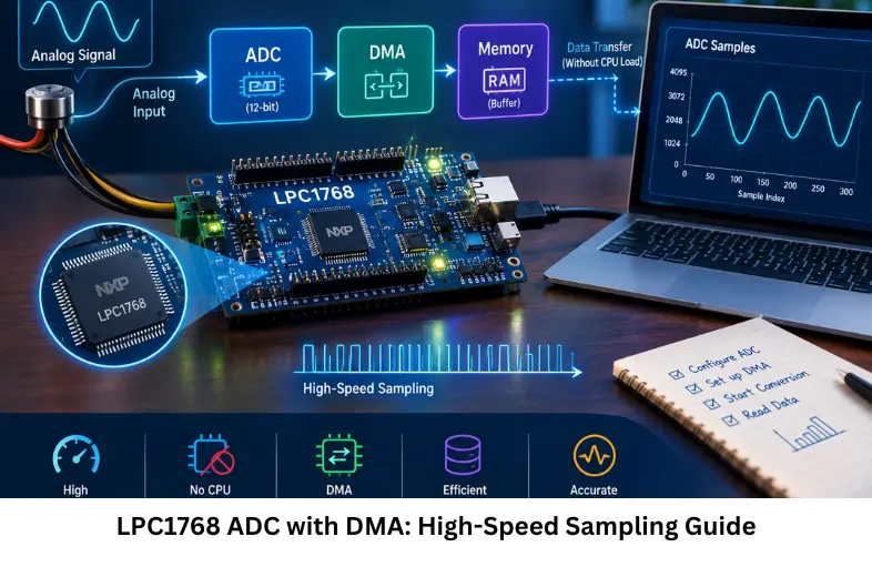
Learn LPC1768 ADC with DMA, 12-bit ADC sampling, DMA buffers, hardware triggers, interrupts, continuous acquisition and real-time processing. Embedded Tech Development Academy (ETDA).
- LPC1768 ADC with DMA: High-Speed Sampling Guide
-
LPC1768 ADC with DMA: High-Speed Analog Sampling Without CPU Overhead
- Introduction to LPC1768 ADC with DMA
- LPC1768 ADC Architecture
- Why DMA Is Used with ADC
- Configuring LPC1768 ADC for DMA
- DMA Channel Configuration
- ADC Result Register and Data Extraction
- Continuous Sampling and Burst Mode
- DMA Buffer Processing
- Real-Time Audio Sampling
- Practical ADC-DMA Applications
- Important Design Considerations
- Frequently Asked Questions
- Conclusion
LPC1768 ADC with DMA: High-Speed Analog Sampling Without CPU Overhead
Introduction to LPC1768 ADC with DMA
Analog-to-digital conversion is a core function in modern embedded systems, where sensors continuously produce analog signals that must be converted into digital data. Applications such as audio acquisition, motor monitoring, power measurement, vibration analysis, industrial instrumentation, and Internet of Things (IoT) devices can generate large numbers of ADC samples. Reading every conversion through CPU polling creates unnecessary processor overhead, while interrupting the CPU for every sample can increase interrupt load and timing jitter.
The LPC1768 ADC with DMA architecture solves this problem by allowing the ADC conversion data to be transferred automatically into SRAM. Direct Memory Access (DMA) performs the repetitive data movement while the CPU concentrates on signal processing, control algorithms, communication, and application tasks.
Important concepts include 12-bit successive-approximation ADC, ADC channels, ADC clock, sampling frequency, burst mode, hardware triggering, DMA request signals, SRAM buffers, transfer width, transfer count, terminal-count interrupts, double buffering, and real-time signal processing.
The LPC1768 provides an 8-channel, 12-bit ADC. The achievable conversion rate depends on ADC clock configuration, conversion timing, trigger method, and device operating conditions. Therefore, sampling-rate claims should always be checked against the LPC1768 datasheet rather than assuming a universal burst-mode rate.
For engineers developing practical embedded systems, ADC and DMA knowledge is highly valuable. Embedded Tech Development Academy (ETDA) provides practical exposure to microcontrollers, embedded C, ADC programming, DMA, timers, and real-time firmware. Learners searching for a Top Embedded Training Institute in Bangalore can develop practical embedded skills with assured placement support.
LPC1768 ADC Architecture
12-Bit Successive-Approximation ADC
The LPC1768 uses a 12-bit successive-approximation ADC with multiple multiplexed analog input channels.
ADC Resolution
A 12-bit ADC produces:
2^12 = 4096 levels
Digital range = 0 to 4095
ADC Conversion Equation
For an ideal ADC:
ADC Code ≈ (Vin / Vref) × 4095Actual accuracy depends on reference voltage, input impedance, electrical noise, PCB layout, and ADC characteristics.
Why DMA Is Used with ADC
CPU Polling Method
With polling, firmware repeatedly checks whether conversion has completed and then reads the ADC result.
Processing Limitation
while (!(LPC_ADC->ADGDR & (1U << 31)))
{
    /* Wait */
}

sample = (LPC_ADC->ADGDR >> 4) & 0xFFF;
DMA-Based Acquisition
With DMA, the ADC generates a DMA request when conversion data becomes available. The DMA controller transfers the configured data to an SRAM buffer without requiring software to perform every copy.
ADC
 ↓
DMA Controller
 ↓
SRAM Buffer
 ↓
CPU Signal Processing
This architecture reduces CPU overhead and is useful for continuous data acquisition.
Configuring LPC1768 ADC for DMA
ADC and DMA Initialization
The required peripheral power and GPIO configuration must be enabled before starting acquisition.
Basic ADC Configuration
#define ADC_CHANNEL 0

void configure_adc(void)
{
    LPC_ADC->ADCR =
        (1U << ADC_CHANNEL) |
        (4U << 8) |
        (1U << 21);       /* DMA enable */

    LPC_ADC->ADINTEN = 0;
}
Pin Multiplexing
The selected GPIO must be configured for the corresponding ADC alternate function. The exact pin assignment should always be verified using the LPC1768 datasheet and the target development board schematic.
DMA Channel Configuration
Source and Destination
For ADC acquisition, the ADC data register acts as the DMA source and an SRAM array acts as the destination.
Transfer Parameters
A DMA configuration normally defines:
- Source address
- Destination address
- Transfer count
- Source width
- Destination width
- Source increment
- Destination increment
- Peripheral request
- Transfer completion interrupt
Conceptual Configuration
DMA_Channel->SRCADDR  = (uint32_t)&ADC_RESULT;
DMA_Channel->DESTADDR = (uint32_t)adc_buffer;

DMA_Channel->CONTROL =
    TRANSFER_COUNT(1024) |
    SRC_WIDTH_16BIT |
    DST_WIDTH_16BIT |
    SRC_FIXED |
    DST_INCREMENT |
    TERMINAL_COUNT_INT;
The exact register fields must match the LPC17xx CMSIS/device header and the selected DMA configuration.
ADC Result Register and Data Extraction
Global Data Register
The ADC global data register contains conversion information together with status and channel-identification bits.
Extracting the Conversion Result
For the LPC17xx ADC data format, firmware typically extracts the conversion value from the defined result field rather than treating the complete 32-bit register as the ADC sample.
Example Extraction
uint16_t sample;

sample = (LPC_ADC->ADGDR >> 4) & 0x0FFF;
The exact DMA transfer strategy should therefore be designed according to the ADC register format and required buffer representation.
Continuous Sampling and Burst Mode
Burst Conversion
Burst mode allows ADC conversions to proceed automatically according to the ADC configuration.
Continuous Acquisition
LPC_ADC->ADCR &= ~(1U << 24);  /* Disable software START */
LPC_ADC->ADCR |=  (1U << 16);  /* Enable BURST */
Deterministic Sampling
For applications requiring an accurate sampling interval, such as audio or waveform measurement, a suitable hardware trigger is preferable where supported. Timer-controlled acquisition provides more deterministic timing than software-controlled conversion loops.
DMA Buffer Processing
Terminal-Count Interrupt
void DMA_IRQHandler(void)
{
    if (LPC_GPDMA->INTTCSTAT & (1U << 0))
    {
        LPC_GPDMA->INTTCCLEAR = (1U << 0);
        dma_complete = 1;
    }
}
Timer Trigger
A hardware timer can generate a periodic event that triggers ADC conversion.
Timer Match
     ↓
ADC Conversion
     ↓
DMA Transfer
     ↓
SRAM Buffer
     ↓
Audio Processing
Block-Based Signal Processing
Once a buffer is complete, firmware can perform:
- Moving-average filtering
- RMS calculation
- Peak detection
- FFT processing
- Threshold detection
- Sensor calibration
- Digital filtering
Block processing reduces the need for CPU intervention on every individual sample.
Real-Time Audio Sampling
Timer-Driven Acquisition
Audio applications require a stable sampling frequency. A common example is 44.1 kHz.
Acquisition Pipeline
Timer Trigger
     ↓
ADC Conversion
     ↓
DMA Transfer
     ↓
SRAM Buffer
     ↓
Audio Processing
Double Buffering
Double buffering allows the CPU to process one block while DMA fills another:
Buffer A → CPU Processing
Buffer B → DMA Acquisition

Buffer B → CPU Processing
Buffer A → DMA Acquisition
This approach helps maintain continuous acquisition and minimizes processing gaps.
Practical ADC-DMA Applications
Sensor Data Acquisition
ADC DMA is useful for temperature, pressure, vibration, current, voltage, and other analog sensors.
Power Monitoring
Continuous voltage and current samples can be collected into SRAM and processed to calculate electrical parameters.
Industrial Data Acquisition
Motor vibration, waveform analysis, fault detection, and instrumentation can benefit from buffered ADC acquisition.
Internet of Things (IoT)
In Internet of Things (IoT) devices, DMA can collect sensor samples while the CPU performs filtering, decision-making, and network communication.
Important Design Considerations
Buffer Size
A larger DMA buffer reduces interrupt frequency but consumes more SRAM and increases processing latency.
ADC Clock
Conversion Timing
The ADC clock must remain within the limits specified by the device documentation. ADC clock configuration directly affects conversion timing and sampling performance.
Sampling Rate
The actual sampling frequency depends on ADC conversion cycles, ADC clock, trigger configuration, and operating conditions.
DMA Debugging
Incorrect source addresses, destination addresses, transfer widths, peripheral requests, or memory configuration can cause DMA failures. Debugging should verify DMA status registers, transfer counters, peripheral configuration, and buffer contents.
Frequently Asked Questions
Why use DMA with the LPC1768 ADC?
DMA automatically transfers ADC conversion data into SRAM, reducing CPU intervention and making continuous data acquisition more efficient.
What is the ADC resolution of the LPC1768?
The LPC1768 contains a 12-bit ADC, providing 4096 theoretical conversion levels from 0 to 4095.
Can LPC1768 ADC DMA be used for audio?
Yes. ADC samples can be transferred into SRAM buffers using DMA, while the CPU processes completed blocks. Timer-based triggering can provide controlled sampling intervals.
Why are SRAM buffers used?
SRAM provides runtime read/write storage suitable for DMA data acquisition. The selected memory region must be compatible with the DMA controller.
What is double buffering?
Double buffering uses two memory buffers so that DMA can fill one buffer while the CPU processes the other, helping maintain continuous acquisition.
Conclusion
The LPC1768 ADC with DMA provides an efficient hardware architecture for continuous analog data acquisition in real-time embedded systems. Instead of polling every conversion or generating software activity for every individual sample, DMA can transfer ADC data into SRAM with minimal CPU intervention. This leaves processor resources available for filtering, control algorithms, communication, diagnostics, and application logic.
Understanding 12-bit ADC conversion, ADC clock configuration, sampling frequency, hardware triggering, burst mode, DMA requests, source and destination addresses, transfer width, SRAM buffers, terminal-count interrupts, buffer management, and double buffering is essential for reliable ADC-DMA firmware.
For engineers working with sensor acquisition, audio processing, power monitoring, industrial instrumentation, and Internet of Things (IoT) devices, these techniques provide a practical foundation for building responsive data-processing systems. Embedded Tech Development Academy (ETDA) focuses on practical embedded C, ARM microcontrollers, ADC programming, DMA, timers, interrupts, and real-time firmware development.
Learners looking for a Top Embedded Training Institute in Bangalore can gain practical experience by implementing ADC acquisition, configuring DMA buffers, analyzing conversion data, and developing real-time firmware. Embedded Tech Development Academy (ETDA) combines practical embedded learning with assured placement support, helping learners develop industry-oriented embedded systems skills.
A structured technical approach is to begin with single-channel ADC conversion, progress to DMA-based buffer acquisition, then implement timer-triggered sampling and double buffering. This progression helps engineers understand the complete hardware-software data path. For learners seeking a Top Embedded Training Institute in Bangalore, practical projects involving ADC, DMA, timers, SRAM, and signal processing can strengthen real-world firmware skills with assured placement support.
As Internet of Things (IoT) and data-intensive embedded applications continue to expand, efficient peripheral-to-memory data movement becomes increasingly important. Embedded Tech Development Academy (ETDA) provides practical exposure to these technologies, while a Top Embedded Training Institute in Bangalore environment can help learners develop hands-on embedded systems knowledge with assured placement support. Mastering LPC1768 ADC with DMA therefore provides a strong technical foundation for high-efficiency data acquisition and real-time firmware development.
Author: ETDA Trainers
Experience: 10+ Years of Industry Experience in Embedded Systems, IoT, and Embedded C Programming