
PCB Design: Complete Guide to Modern PCB Design & Manufacturing
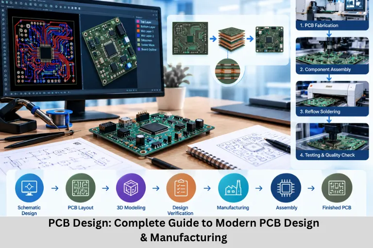
Learn PCB design fundamentals, schematic capture, PCB layout, signal integrity, power integrity, HDI, RF design, DFM, simulation, and future PCB technologies. Embedded Tech Development Academy (ETDA).
- PCB Design: Complete Guide to Modern PCB Design & Manufacturing
-
PCB Design: The Art and Science of Modern Electronics Manufacturing
- Introduction to PCB Design
- 1. Schematic Design
- 2. PCB Board Layout
- Key PCB Design Considerations
- Manufacturing and Assembly Considerations
- Modern PCB Technologies
- PCB Design Tools and Engineering Methodologies
- Major Challenges in PCB Design
- Future Trends in PCB Design
- Frequently Asked Questions
- Conclusion
PCB Design: The Art and Science of Modern Electronics Manufacturing
Introduction to PCB Design
Printed Circuit Board (PCB) design is the foundation of modern electronics manufacturing, transforming an electrical circuit from a conceptual schematic into a reliable physical product. Almost every electronic system, including smartphones, automotive ECUs, medical devices, industrial controllers, Internet of Things (IoT) devices, aerospace systems, computers, and communication equipment, depends on a properly engineered PCB.
PCB design involves much more than placing components and connecting traces. A professional PCB designer must consider schematic capture, component selection, PCB layout, signal integrity, power integrity, impedance control, thermal management, electromagnetic interference (EMI), electromagnetic compatibility (EMC), manufacturability, assembly, reliability, and testing. The PCB must electrically perform as intended while also satisfying mechanical and manufacturing constraints.
Modern electronic circuit design, multilayer PCB design, high-speed PCB layout, RF PCB design, embedded hardware design, PCB manufacturing, Design for Manufacturing (DFM), Design for Assembly (DFA), and hardware verification increasingly require engineers to understand both electrical theory and manufacturing technology.
For engineers developing these practical skills, Embedded Tech Development Academy (ETDA) provides industry-oriented technical learning covering embedded hardware, electronics, microcontrollers, PCB concepts, and practical engineering workflows. Learners searching for a Top Embedded Training Institute in Bangalore can benefit from hands-on technical exposure and assured placement support. PCB designF knowledge is particularly valuable for embedded engineers because the PCB forms the physical platform connecting processors, sensors, power supplies, communication interfaces, and peripheral circuits.
1. Schematic Design
Major Power Conversion Types
The schematic represents the logical electrical connection of the circuit before physical layout begins.
Key activities include:
- Circuit conceptualization using EDA tools such as Altium Designer, KiCad, and Cadence tools
- Component selection and datasheet verification
- Symbol and footprint library management
- Net naming and connectivity definition
- Electrical Rule Checking (ERC)
Component and Footprint Verification
A component footprint must accurately match the manufacturer’s package dimensions, pin numbering, pad geometry, courtyard, and assembly requirements. Incorrect footprints can cause serious manufacturing or assembly failures.
Electrical Rule Checking
ERC identifies problems such as unconnected pins, incorrect electrical connections, power-input errors, and unintended net relationships before PCB layout begins.
2. PCB Board Layout
PCB layout converts the schematic into a physical arrangement of components, copper traces, planes, vias, and mechanical features.
Placement should consider signal flow, thermal behavior, component accessibility, noise coupling, power distribution, and mechanical constraints.
Critical Signal Routing
High-speed signals, clocks, differential pairs, RF paths, and power nets require specialized routing techniques. Trace width, spacing, layer transitions, reference planes, and return-current paths directly influence electrical performance.
Design Rule Checking
DRC verifies spacing, trace widths, clearances, via sizes, component constraints, and other manufacturing rules before fabrication files are generated.
Key PCB Design Considerations
Signal Integrity
Signal integrity becomes increasingly important as digital interfaces operate at higher data rates.
Important techniques include:
- Controlled impedance routing
- Microstrip and stripline structures
- Differential-pair routing
- Length matching
- Crosstalk reduction
- Via optimization
- Proper return-current paths
Impedance Control
Controlled impedance ensures that high-speed transmission lines maintain the required characteristic impedance. Stackup parameters such as dielectric thickness, trace width, copper thickness, and dielectric constant influence impedance.
Differential Pair Design
Interfaces such as USB, Ethernet, PCIe, and high-speed memory use differential signaling. Maintaining appropriate pair spacing, length matching, reference planes, and routing symmetry helps minimize timing and signal-integrity problems.
Power Integrity
A stable power-delivery network is essential for processors, FPGAs, memory devices, analog circuits, and communication ICs.
Designers must consider:
- Power and ground planes
- Decoupling capacitors
- Voltage drop
- Current density
- PDN impedance
- Return-current paths
Decoupling Capacitor Placement
Decoupling capacitors should generally be positioned close to IC power pins to reduce parasitic inductance and provide a low-impedance high-frequency current path.
Power Distribution Network
PDN analysis helps determine whether supply impedance, voltage ripple, transient response, and resonance remain within acceptable limits during dynamic load conditions.
Thermal Management
Heat generation affects PCB reliability and component lifetime.
Design techniques include:
- Appropriate copper weight
- Thermal vias
- Copper pours
- Heat sinks
- Thermal relief optimization
- Component spacing
Thermal Via Design
Thermal vias transfer heat from component pads or exposed thermal regions into internal or bottom copper layers. Their diameter, pitch, number, and connection to copper structures influence thermal performance.
Manufacturing and Assembly Considerations
Design for Manufacturing
Design for Manufacturing (DFM) ensures that a PCB can be fabricated consistently within the capabilities of the manufacturing process.
DFM parameters include:
- Minimum trace width
- Minimum spacing
- Drill diameter
- Annular ring
- Copper-to-edge clearance
- Layer registration
- Solder-mask requirements
Design for Assembly
DFA focuses on efficient and reliable component assembly. Component orientation, spacing, polarity markings, solder-joint accessibility, and pick-and-place requirements must be considered.
Testability
A production-ready PCB should support electrical testing through:
- Test points
- Boundary scan
- In-circuit testing
- Functional testing
- Programming/debug interfaces
Modern PCB Technologies
High-Density Interconnect PCBs
HDI PCBs support high component density using technologies such as microvias, fine traces, sequential lamination, and advanced multilayer structure
Microvia Technology
Laser-drilled microvias connect adjacent layers and allow dense routing beneath fine-pitch packages such as BGAs.
Fine-Pitch Component Routing
Fine-pitch packages require precise escape routing, controlled clearances, optimized via structures, and accurate fabrication processes.
Flexible and Rigid-Flex PCBs
Flexible PCBs are used where weight, space, or mechanical movement is important.
Design considerations include:
- Bend radius
- Copper geometry
- Dynamic flexing
- Stiffener placement
- Material selection
High-Speed PCB Design
High-speed designs require careful control of transmission-line behavior, dielectric properties, impedance, propagation delay, and signal reflections.
Backdrilling can remove unused via stubs that otherwise cause signal discontinuities at high frequencies.
RF and Microwave PCB Design
RF boards require specialized transmission-line structures, controlled impedance, grounding, shielding, antenna integration, and electromagnetic simulation.
PCB Design Tools and Engineering Methodologies
ECAD Software
Professional PCB development uses Electronic Computer-Aided Design tools for schematic capture, layout, simulation, libraries, manufacturing outputs, and design-rule management.
Common platforms include Altium Designer, Cadence Allegro, and KiCad.
Simulation and Analysis
Advanced designs may use:
- 3D electromagnetic simulation
- Signal-integrity analysis
- Power-integrity simulation
- Thermal modeling
- Mechanical analysis
- Vibration analysis
Version Control
Hardware development increasingly uses version-control concepts similar to software development.
Hardware Revision Management
Engineers can track schematic revisions, PCB revisions, component substitutions, design changes, manufacturing outputs, and documentation.
Team Collaboration
Structured revision management prevents outdated fabrication files from being released and improves collaboration between hardware, firmware, manufacturing, and testing teams.
Major Challenges in PCB Design
Miniaturization
Modern products use packages such as 01005, CSP, QFN, and fine-pitch BGA, requiring extremely dense routing and precise manufacturing.
High-Speed Complexity
Interfaces such as DDR5 and PCIe require careful attention to timing, impedance, insertion loss, return paths, crosstalk, and power integrity.
Supply Chain Constraints
Component obsolescence, availability, lead times, lifecycle status, and alternate components increasingly influence PCB design decisions.
Environmental Compliance
PCB manufacturing must consider requirements involving RoHS, REACH, halogen-free materials, material selection, and sustainable electronics manufacturing.
Future Trends in PCB Design
Embedded Components
Embedding passive components and semiconductor dies inside PCB structures can reduce board size and improve electrical interconnect performance.
Advanced PCB Materials
Low-loss laminates are increasingly important for high-frequency applications, while thermally conductive substrates can improve heat transfer.
AI-Assisted PCB Design
AI-based tools are emerging for routing optimization, component placement, design-rule recommendations, constraint analysis, and potential failure prediction.
3D Printed Electronics
Additive manufacturing can create conductive traces and complex electronic structures using conductive inks and specialized materials.
Frequently Asked Questions
What is PCB design?
PCB design is the process of converting an electronic circuit schematic into a physical board containing components, copper traces, planes, vias, and mechanical features.
What are the main stages of PCB design?
The major stages include schematic capture, component and footprint selection, board layout, signal and power analysis, design verification, DFM/DFA checks, and manufacturing-file generation.
Why is signal integrity important in PCB design?
Signal integrity ensures that electrical signals reach their destinations with acceptable voltage levels, timing, impedance, noise, and waveform quality. It becomes particularly important in high-speed digital and RF systems.
What is HDI PCB technology?
High-Density Interconnect PCB technology uses microvias, fine traces, advanced multilayer structures, and sequential lamination to achieve high routing density in compact electronic products.
Is PCB design important for embedded systems engineers?
Yes. Embedded engineers work with microcontrollers, sensors, communication interfaces, power supplies, and peripheral circuits that must be physically integrated on PCBs. Understanding PCB layout helps engineers identify hardware constraints and design reliable embedded products.
Conclusion
PCB design is the critical engineering bridge between electronic circuit concepts and manufacturable hardware. A successful PCB must satisfy multiple requirements simultaneously: electrical performance, mechanical constraints, thermal behavior, manufacturability, assembly, testability, reliability, and regulatory requirements. From schematic capture and component selection to high-speed routing, impedance control, power integrity, thermal management, EMI/EMC analysis, DFM, DFA, and manufacturing documentation, every stage influences the final product.
As electronics continue to become smaller, faster, and more interconnected, technologies such as HDI PCBs, microvias, rigid-flex circuits, advanced PCB laminates, RF/microwave design, embedded components, AI-assisted PCB layout, and 3D printed electronics will become increasingly important. Engineers must therefore develop a strong understanding of electronic hardware design, PCB manufacturing, signal integrity, power integrity, embedded hardware, high-speed design, and design verification.
For students and professionals seeking practical expertise in embedded hardware and electronics, Embedded Tech Development Academy (ETDA) provides industry-oriented technical training with hands-on learning. As a Top Embedded Training Institute in Bangalore, ETDA helps learners strengthen their understanding of embedded systems, microcontrollers, electronics, PCB concepts, and hardware development while offering assured placement support.
Building practical skills through Embedded Tech Development Academy (ETDA) can help aspiring engineers understand how firmware, microcontrollers, sensors, power circuits, communication interfaces, and PCB hardware work together in real products. For candidates looking for a Top Embedded Training Institute in Bangalore, Embedded Tech Development Academy (ETDA) combines technical learning, practical project exposure, and assured placement support to prepare learners for modern embedded and electronics engineering careers.
Author: ETDA Trainers
Experience: 10+ Years of Industry Experience in Embedded Systems, IoT, and Embedded C Programming