
Single Stage Common Emitter Amplifier: BJT CE Guide
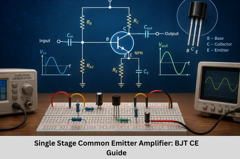
Learn single-stage common emitter amplifier design, BJT biasing, voltage gain, small-signal analysis, frequency response, stability, and applications. Embedded Tech Development Academy. (ETDA).
- Single Stage Common Emitter Amplifier: BJT CE Guide
-
Single Stage Common Emitter Amplifier: The Fundamental BJT Configuration
- Introduction to Common Emitter Amplifier
- Circuit Configuration
- DC Biasing Analysis
- AC Small-Signal Analysis
- Frequency Response of CE Amplifier
- Practical CE Amplifier Design
- Simulation and Expected Results
- Performance Optimization
- Practical Applications
- Troubleshooting Guide
- Measurement Procedure
- Frequently Asked Questions
- Conclusion
Single Stage Common Emitter Amplifier: The Fundamental BJT Configuration
Introduction to Common Emitter Amplifier
The Common Emitter (CE) amplifier is one of the most important and widely used configurations of a Bipolar Junction Transistor (BJT). It is commonly studied in analog electronics because it provides significant voltage gain, current gain, and power gain while maintaining a practical input and output impedance. The emitter terminal is common to both the input and output circuits, while the input is applied between the base and emitter and the output is taken between the collector and emitter.
A single-stage CE amplifier is a fundamental building block in transistor amplifier design, analog circuit design, sensor signal conditioning, audio amplification, and embedded hardware interfaces. Understanding its DC biasing, Q-point selection, small-signal model, frequency response, and gain calculations is essential for engineers working with electronic circuits.
For students learning embedded systems and embedded hardware design, the CE amplifier provides a strong foundation for understanding how weak sensor signals can be amplified before being processed by an ADC or microcontroller. At Embedded Tech Development Academy (ETDA), practical electronics concepts such as BJT operation, amplifier circuits, analog interfacing, and embedded circuit design can help students connect theoretical electronics with real-world hardware development. As a Top Embedded Training Institute in Bangalore, Embedded Tech Development Academy (ETDA) focuses on technical learning through practical concepts, projects, and industry-oriented training with assured placement support.
Key Characteristics of CE Amplifier
The main characteristics of a single-stage common emitter amplifier include:
Voltage and Current Gain
A CE amplifier provides significant voltage gain and current gain, making it suitable for amplifying weak electrical signals.
Phase Inversion
The output signal is approximately 180° out of phase with the input signal.
Input and Output Impedance
The CE configuration generally provides moderate input and output impedance, making it suitable for many general-purpose amplifier applications.
Important CE Amplifier Parameters
- Medium to high voltage gain
- Moderate input impedance
- Moderate output impedance
- 180° phase shift
- Good current gain
- Useful frequency response
- Simple circuit implementation
Importance in Embedded Electronics
The CE amplifier is particularly useful for understanding analog front-end circuits and sensor interfaces in embedded systems. Many sensors generate low-amplitude analog signals that may require amplification before being supplied to an ADC or microcontroller.
At Embedded Tech Development Academy (ETDA), understanding fundamental analog electronics concepts such as BJT operation, amplifier circuits, signal conditioning, and embedded hardware design helps students connect theoretical electronics with practical embedded applications. As a Top Embedded Training Institute in Bangalore, Embedded Tech Development Academy (ETDA) emphasizes practical technical learning, real-world projects, and assured placement support for aspiring embedded engineers.
Circuit Configuration
Basic CE Amplifier Structure
A typical single-stage CE amplifier consists of:
Main Circuit Components
- BJT transistor
- Collector resistor (Rc)
- Emitter resistor (Re)
- Voltage-divider resistors (R1 and R2)
- Input coupling capacitor (Cin)
- Output coupling capacitor (Cout)
- Emitter bypass capacitor (Ce)
- DC supply (Vcc)
Function of the Bias Network
The voltage-divider network establishes the transistor’s base voltage. The emitter resistor provides DC and thermal stability, while the collector resistor converts collector-current variations into output-voltage variations.
Typical Component Values
| Component | Role | Typical Value |
|---|---|---|
| R1, R2 | Voltage divider | 10 kΩ–100 kΩ |
| RC | Collector resistor | 1 kΩ–10 kΩ |
| RE | Emitter resistor | 100 Ω–1 kΩ |
| Cin, Cout | Coupling capacitors | 1 µF–10 µF |
| Ce | Emitter bypass capacitor | 10 µF–100 µF |
DC Biasing Analysis
Voltage Divider Bias Equations
The base voltage is approximately:
Vb = Vcc × R2/(R1 + R2)
The emitter voltage is:
Ve = Vb − Vbe
For a silicon BJT:
Vbe ≈ 0.7 V
The emitter current is:
Ie = Ve/Re ≈ Ic
Collector-emitter voltage is:
Vce = Vcc − Ic(Rc + Re)
Q-Point and Bias Stability
The objective of transistor biasing is to establish a suitable Q-point so that the BJT remains in the active region during signal amplification.
Stability Factor
A commonly used stability-factor expression is:
S = (1 + β) / [1 + β(Re/(Re + Rth))]
where:
Rth = R1 || R2
Stability Principle
A lower stability factor generally indicates improved resistance to transistor parameter and temperature variations.
Example DC Calculation
Given:
- Vcc = 12 V
- R1 = 68 kΩ
- R2 = 12 kΩ
- Re = 1 kΩ
- β = 100
Therefore:
Vb = 12 × 12/(68 + 12) = 1.8 V
Ve = 1.8 − 0.7 = 1.1 V
Ie = 1.1 V/1 kΩ = 1.1 mA
Thus:
Ic ≈ 1.1 mA
For Rc = 4.7 kΩ:
Vce = 12 − 1.1 mA(4.7 kΩ + 1 kΩ)
Vce ≈ 5.73 V
This places the transistor in a useful active-region operating point.
AC Small-Signal Analysis
Small-Signal Model Parameters
At midband frequencies, the transistor can be represented using a small-signal model.
| Parameter | Formula | Typical Range |
|---|---|---|
| re | 25 mV / Ie | 5–50 Ω |
| gm | Ic / 25 mV | 10–100 mS |
| β | ΔIc / ΔIb | 50–300 |
| rin | βre | 500 Ω–15 kΩ |
Voltage Gain
Without Emitter Bypass Capacitor
Av = −Rc/(re + Re)
The emitter resistor introduces negative feedback and reduces voltage gain while improving stability.
With Emitter Bypass Capacitor
When Ce effectively bypasses Re:
Av = −Rc/re
Phase Relationship
The negative sign indicates that the CE amplifier produces approximately 180° phase inversion between input and output.
Input and Output Impedance
Without Ce:
Zin = R1 || R2 || β(re + Re)
With Ce:
Zin = R1 || R2 || βre
The approximate output impedance is:
Zout ≈ Rc
In practical circuits, the load resistance must also be considered when determining effective collector loading.
Frequency Response of CE Amplifier
Low-Frequency Response
At low frequencies, coupling and bypass capacitors introduce significant reactance.
The approximate input cutoff frequency is:
fL ≈ 1/[2πCin(Rs + Zin)]
The output cutoff can be estimated as:
fL ≈ 1/[2πCout(Rc + RL)]
High-Frequency Response
At high frequencies, transistor junction capacitances and stray capacitances become significant.
The high-frequency cutoff can be approximated by:
fH ≈ 1/[2π(Rc || RL)Cout]
where effective capacitance includes transistor capacitances such as Cbe and Cbc, along with parasitic capacitance.
Miller Effect
The collector-base capacitance contributes to the Miller effect, which can significantly reduce the high-frequency bandwidth of a common emitter amplifier.
Gain-Bandwidth Trade-Off
Increasing amplifier gain can reduce bandwidth, creating an important trade-off in practical transistor amplifier design.
Gain-Bandwidth Product
GBW = |Av| × BW
where:
BW = fH − fL
Practical CE Amplifier Design
Design Specifications
Consider:
- Vcc = 12 V
- Ic = 1 mA
- Av = −100
- β = 100
- RL = 10 kΩ
- Rs = 1 kΩ
Collector Resistor Calculation
For Ic = 1 mA:
re ≈ 25 Ω
Using:
|Av| = Rc/re
Therefore:
100 = Rc/25
Rc = 2.5 kΩ
A practical standard value such as 2.7 kΩ can be selected after verifying the required Q-point and output swing.
Emitter Resistor Calculation
Choosing:
Ve ≈ Vcc/10 = 1.2 V
gives:
Re = 1.2 V/1 mA = 1.2 kΩ
Bias Resistor Calculation
Base voltage:
Vb = Ve + 0.7 = 1.9 V
Using an appropriate divider current, practical resistor values can be selected around:
R1 = 91 kΩ
R2 = 18 kΩ
These values should be verified against the actual transistor β and desired operating point.
Emitter Bypass Capacitor
For a target low-frequency response near 100 Hz:
XCe << Re
Therefore:
Ce >> 1/(2πfRe)
A practical value such as 10 µF may be selected depending on the desired gain and cutoff frequency.
Simulation and Expected Results
Input and Output Waveforms
For a 10 mVpp, 1 kHz sine-wave input, a CE amplifier designed for approximately −100 voltage gain could theoretically produce around 1 Vpp output, provided the transistor remains within its linear operating region.
Output Phase
The output waveform is inverted by approximately 180° relative to the input.
Frequency Response
A representative design may provide:
- Midband gain: approximately 40 dB
- Low cutoff: approximately 80–100 Hz
- High cutoff: approximately 150 kHz
Actual performance depends on transistor characteristics, biasing, capacitor values, source resistance, load resistance, and parasitic capacitances.
Performance Optimization
Increasing Voltage Gain
Voltage gain can be increased by:
- Increasing effective collector load
- Using an active current-source load
- Properly bypassing the emitter resistor
- Using a cascode configuration
Improving Bandwidth
Bandwidth can be improved using:
- Lower collector resistance
- Appropriate transistor selection
- Reduced parasitic capacitance
- Emitter degeneration
- Cascode configurations
- Optimized PCB layout
Improving Stability
Amplifier stability can be improved through:
Bias and Feedback Techniques
- Emitter degeneration
- Negative feedback
- Proper DC biasing
- Thermal compensation
- Supply decoupling
PCB-Level Considerations
Good grounding, short signal paths, proper decoupling, and controlled parasitic capacitance are important when implementing high-gain amplifier circuits on a PCB.
Practical Applications
CE amplifiers are used in:
- Microphone preamplifiers
- Audio preamplifier stages
- Tone-control circuits
- Small-signal audio circuits
Sensor Interfaces
They can be used for signal conditioning with:
- Photodiodes
- Temperature sensors
- Strain gauges
- Other low-level analog sensors
RF and Communication Circuits
CE transistor stages can also be found in:
- Intermediate-frequency amplifiers
- Modulator stages
- Demodulator circuits
- RF gain stages
Troubleshooting Guide
Common Problems
| Problem | Possible Cause | Solution |
|---|---|---|
| No output | Incorrect biasing | Check Q-point and VCE |
| Distortion | Incorrect Q-point | Adjust bias network |
| Low gain | Incorrect Ce or loading | Check bypass capacitor and load |
| Oscillation | Poor grounding/decoupling | Improve layout and supply bypassing |
Measurement Procedure
Recommended Testing Sequence
- Measure DC voltages before applying the AC signal.
- Verify collector, base, and emitter voltages.
- Confirm that the transistor operates in the active region.
- Apply a small AC input.
- Observe input and output waveforms using an oscilloscope.
- Increase input amplitude gradually.
- Check for clipping and waveform distortion.
Important Measurement Rule
Always verify the DC operating point before performing AC gain measurements, because incorrect biasing can produce misleading amplifier results.
Frequently Asked Questions
What Is a Common Emitter Amplifier?
A common emitter amplifier is a BJT amplifier configuration in which the emitter is common to the input and output circuits. It provides significant voltage and current gain with approximately 180° phase inversion.
Why Does a CE Amplifier Invert the Signal?
An increase in base current increases collector current. This increases the voltage drop across Rc and reduces collector voltage. Therefore, the output voltage changes in the opposite direction to the input voltage.
What Is the Function of the Emitter Bypass Capacitor?
The emitter bypass capacitor provides a low-impedance AC path around Re. This reduces AC negative feedback and increases voltage gain while allowing Re to provide DC bias stabilization.
Why Is Voltage Divider Bias Used?
Voltage-divider bias establishes a relatively stable base voltage and reduces the effect of transistor β variations. Together with emitter resistance, it improves Q-point stability.
What Limits CE Amplifier Bandwidth?
At low frequencies, coupling and bypass capacitors affect the response. At high frequencies, transistor junction capacitances, stray capacitances, and the Miller effect limit bandwidth.
Conclusion
The single-stage Common Emitter amplifier is a fundamental circuit for understanding BJT amplifier design, transistor biasing, small-signal analysis, voltage gain, impedance, frequency response, and analog signal amplification. Its combination of voltage gain and current gain makes it valuable in audio circuits, sensor interfaces, communication systems, and embedded electronics.
A proper CE amplifier design requires more than simply selecting resistor values. Engineers must establish a stable DC operating point, maintain the transistor in its active region, calculate small-signal parameters, consider loading effects, select appropriate coupling and bypass capacitors, and evaluate both low- and high-frequency limitations. Practical factors such as thermal stability, PCB parasitics, grounding, decoupling, and transistor tolerances also influence real-world performance.
For engineers preparing for careers in embedded electronics, mastering the CE amplifier builds a strong foundation for analog electronics, embedded hardware design, sensor interfacing, signal conditioning, and mixed-signal systems. Embedded Tech Development Academy (ETDA) emphasizes industry-oriented technical learning that connects such electronics fundamentals with practical embedded systems development. As a Top Embedded Training Institute in Bangalore, Embedded Tech Development Academy (ETDA) provides structured technical training, hands-on learning, project exposure, and assured placement support to help learners develop job-ready embedded skills.
For students and aspiring embedded engineers looking to strengthen their understanding of transistor circuits and practical hardware development, learning these fundamentals through an industry-focused program at Embedded Tech Development Academy (ETDA) can provide a useful pathway toward embedded engineering careers. Embedded Tech Development Academy (ETDA), recognized as a Top Embedded Training Institute in Bangalore, combines technical concepts with practical development and assured placement support, helping learners move from electronics fundamentals toward real-world embedded system design.
Author: ETDA Trainers
Experience: 10+ Years of Industry Experience in Embedded Systems, IoT, and Embedded C Programming