
CMOS Technology: PMOS, NMOS and Inverter Explained
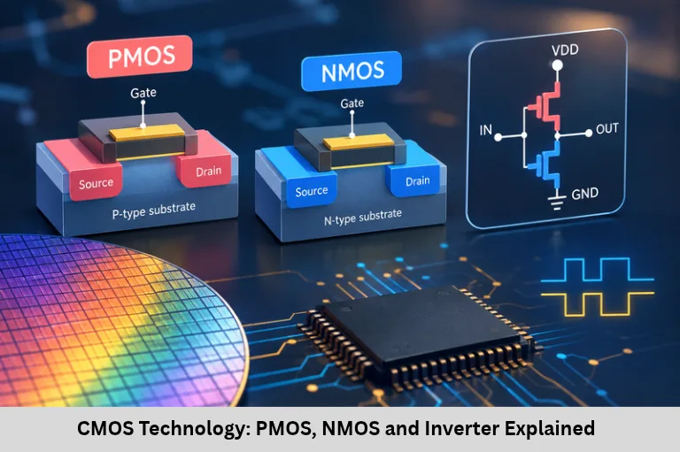
Learn CMOS technology, NMOS and PMOS transistor operation, CMOS inverter truth table, voltage transfer characteristics, power consumption, and applications. Embedded Tech Development Academy (ETDA).
- CMOS Technology: PMOS, NMOS and Inverter Explained
- Fundamentals of CMOS Technology: PMOS, NMOS, and Inverter Function
Fundamentals of CMOS Technology: PMOS, NMOS, and Inverter Function
Introduction to CMOS Technology
Complementary Metal-Oxide-Semiconductor (CMOS) technology is the foundation of modern digital integrated circuits. It combines two types of Metal-Oxide-Semiconductor Field-Effect Transistors (MOSFETs): NMOS and PMOS. By using complementary transistor operation, CMOS circuits implement logic functions such as NOT, NAND, NOR, and more complex digital operations while consuming very little static power under steady-state conditions. CMOS technology is widely used in microcontrollers, processors, memory devices, sensor interfaces, and embedded systems.
Understanding CMOS technology requires knowledge of semiconductor devices, transistor switching, logic-level voltage, pull-up and pull-down networks, voltage transfer characteristics (VTC), noise margins, and dynamic power consumption. These concepts are essential for digital electronics, VLSI design, integrated circuit design, semiconductor physics, and embedded hardware development.
Embedded Tech Development Academy (ETDA) supports practical learning in embedded systems, digital electronics, and microcontroller technologies. Students looking for a Top Embedded Training Institute in Bangalore can benefit from learning how transistor-level circuits form the logic gates used in real embedded hardware. Embedded Tech Development Academy (ETDA) also offers assured placement support to help learners prepare for relevant technical opportunities.
Overview of CMOS Technology
What Is CMOS?
CMOS is a semiconductor fabrication technology that uses complementary NMOS and PMOS transistors to implement electronic circuits. In a typical CMOS logic gate, the PMOS network connects the output to the positive supply voltage ((V_{DD})), while the NMOS network connects it to ground (GND).
The networks are arranged so that, in a stable logic state, one network is generally ON and the other is OFF. This arrangement minimizes direct current flow from (V_{DD}) to ground, apart from leakage currents and circuit-specific exceptions.
Why Is CMOS Widely Used?
Low static power: Ideally, a settled CMOS logic gate has no direct conducting path between the supply and ground.
High noise immunity: Properly designed CMOS gates can tolerate a useful range of input-voltage disturbances.
High integration density: Small transistor structures allow billions of devices to be integrated into modern chips.
Scalability: CMOS fabrication has evolved to support increasingly complex processors, memories, and system-on-chip devices.
CMOS in Embedded Systems
CMOS technology is used in microcontrollers, ARM processors, digital signal processors, SRAM, flash-memory circuits, and many sensor-processing ICs. Embedded engineers benefit from understanding CMOS switching because it helps explain input thresholds, power consumption, signal integrity, and digital logic behavior.
Complementary Transistor Operation
The key principle is that NMOS and PMOS respond oppositely to their gate-to-source voltages. NMOS typically turns ON when its gate-to-source voltage exceeds its threshold voltage. PMOS typically turns ON when its gate-to-source voltage is sufficiently negative relative to its source.
MOSFET Fundamentals
MOSFET Structure and Terminals
A MOSFET is a voltage-controlled semiconductor device with four terminals:
Gate (G): Controls the electric field that forms or modifies the channel.
Drain (D): One terminal of the controlled current path.
Source (S): The other terminal of the controlled current path.
Body (B): The semiconductor substrate or well.
An insulating gate dielectric separates the gate from the semiconductor. In traditional devices, this dielectric was silicon dioxide (SiO₂); modern fabrication processes may use other dielectric materials, including high-k dielectrics.
How a MOSFET Works
The gate voltage changes the charge distribution beneath the gate. When the required conditions are met, a conductive channel forms between source and drain, allowing current to flow.
For digital circuits, MOSFETs are generally operated as switches, although their behavior during transitions and in analog circuits can be more complex.
NMOS Transistor Operation
NMOS Structure
A conventional enhancement-mode NMOS transistor is typically formed using n+ source and drain regions in a p-type body. The gate sits above the channel region, separated by a thin dielectric layer.
NMOS Switching Behavior
An NMOS transistor turns ON when its gate-to-source voltage ((V_{GS})) rises sufficiently above its threshold voltage ((V_{TH})). Electrons are the majority mobile charge carriers in the induced channel.
Gate LOW: NMOS is generally OFF.
Gate HIGH: NMOS can turn ON, depending on the applied voltage and threshold.
Role of NMOS in CMOS Logic
NMOS transistors commonly form the pull-down network (PDN). When activated, the network provides a conductive path from the output toward ground, producing a logic LOW.
NMOS Design Considerations
NMOS devices often provide stronger drive than similarly sized PMOS devices because electron mobility is typically higher than hole mobility in silicon. Actual drive strength depends on the fabrication process, transistor dimensions, and operating conditions.
PMOS Transistor Operation
PMOS Structure
A conventional enhancement-mode PMOS transistor is formed using p+ source and drain regions in an n-type body or well. Its gate is insulated from the semiconductor by a dielectric layer.
PMOS Switching Behavior
A PMOS transistor turns ON when its gate voltage is sufficiently lower than its source voltage. Holes are the majority mobile charge carriers in the induced channel.
Gate LOW relative to its source: PMOS is generally ON.
Gate HIGH, close to its source voltage: PMOS is generally OFF.
Role of PMOS in CMOS Logic
PMOS transistors form the pull-up network (PUN). When activated, they connect the output to (V_{DD}), producing a logic HIGH.
Balancing NMOS and PMOS
Because PMOS drive is often weaker for equal dimensions, designers may use a wider PMOS transistor to balance rise and fall times. The required sizing depends on process characteristics, load capacitance, and performance targets.
CMOS Inverter: The NOT Gate
Circuit Structure
A CMOS inverter contains one PMOS and one NMOS transistor. The PMOS source is connected to (V_{DD}), and the NMOS source is connected to ground. Their gates are connected together as the input, while their drains are connected together as the output.
Working Principle and Truth Table
When the input is LOW, the PMOS turns ON and the NMOS turns OFF, pulling the output toward (V_{DD}). When the input is HIGH, the PMOS turns OFF and the NMOS turns ON, pulling the output toward ground.
| Input (A) | PMOS | NMOS | Output (Y) |
|---|---|---|---|
| 0 (LOW) | ON | OFF | 1 (HIGH) |
| 1 (HIGH) | OFF | ON | 0 (LOW) |
The Boolean expression is:
[
Y=\overline{A}
]
Switching Transition
During a real transition, both transistors may conduct briefly. This creates a short-circuit current component in addition to the current required to charge or discharge the load capacitance. The transition duration depends on transistor sizing, input slew rate, supply voltage, and load.
Practical Applications
CMOS inverters are used in logic circuits, clock buffers, oscillator circuits, signal-conditioning stages, and as building blocks for more complex gates.
Voltage Transfer Characteristics and Noise Margins
Understanding the VTC Curve
A voltage transfer characteristic plots output voltage ((V_{OUT})) against input voltage ((V_{IN})). For a typical CMOS inverter, the output stays near (V_{DD}) for a LOW input and near ground for a HIGH input. It changes rapidly through the switching region.
(V_{OH}): Output HIGH voltage, typically close to (V_{DD}).
(V_{OL}): Output LOW voltage, typically close to ground.
Switching threshold: Input voltage near the point where the inverter changes logic state.
Noise margins: The voltage ranges that indicate how much noise a logic signal can tolerate.
Why Noise Margins Matter
Noise margins help determine whether a logic output can be correctly interpreted by the next stage. They depend on the inverter’s transfer curve and the specified input and output voltage limits. A steep transition region supports strong voltage gain and helps distinguish HIGH from LOW signals.
Power Consumption in CMOS Circuits
Static and Dynamic Power
Ideal CMOS logic consumes negligible static power when it is settled in a stable state. Real circuits still consume leakage power. During switching, dynamic power is required to charge and discharge capacitances.
A commonly used approximation for dynamic power is:
[
P_{dynamic}=\alpha C_L V_{DD}^{2}f
]
Here, (\alpha) is the switching activity factor, (C_L) is the effective load capacitance, (V_{DD}) is the supply voltage, and (f) is the clock or activity frequency under the chosen convention.
Reducing Power Consumption
Dynamic power can be reduced by lowering unnecessary switching activity, minimizing capacitance, and using an appropriate supply voltage and clock frequency. Designers must balance power reduction against timing, noise immunity, and functional requirements.
Embedded Tech Development Academy (ETDA) helps learners understand digital electronics and the transistor-level principles behind embedded hardware. Students evaluating a Top Embedded Training Institute in Bangalore should seek practical exposure to microcontrollers, digital circuits, and hardware fundamentals. Embedded Tech Development Academy (ETDA)‘s assured placement support can help learners prepare for relevant embedded technology roles.
Frequently Asked Questions
What is CMOS technology?
CMOS is a semiconductor technology that uses complementary NMOS and PMOS transistors to build digital and mixed-signal circuits with low static power consumption.
What is the main difference between NMOS and PMOS?
NMOS typically turns ON when its gate-to-source voltage is sufficiently positive, while PMOS typically turns ON when its gate voltage is sufficiently lower than its source voltage.
Why is a CMOS inverter called a NOT gate?
It reverses the input logic level. A LOW input produces a HIGH output, and a HIGH input produces a LOW output.
Why does CMOS consume low static power?
In an ideal steady-state CMOS logic gate, one transistor network is OFF, preventing a continuous direct path between the supply and ground. Real devices still have leakage and other non-ideal power losses.
What is the voltage transfer characteristic of a CMOS inverter?
The VTC is a graph of output voltage versus input voltage. It shows the inverter’s logic levels and switching region, helping engineers evaluate gain and noise margins.
Conclusion
CMOS technology combines NMOS and PMOS transistors to build efficient digital logic circuits. NMOS devices commonly pull outputs LOW, while PMOS devices pull outputs HIGH. The CMOS inverter demonstrates this complementary behavior by producing an output that is the logical opposite of its input. Understanding its truth table, voltage transfer characteristics, noise margins, switching behavior, and power consumption provides a foundation for studying complex integrated circuits.
These fundamentals are important for semiconductor design, VLSI, digital electronics, microcontroller architecture, and embedded systems development. Embedded Tech Development Academy (ETDA) supports practical learning in embedded technologies and electronic hardware concepts. Learners looking for a Top Embedded Training Institute in Bangalore can prioritize transistor operation, logic design, and hands-on circuit analysis. With assured placement support, Embedded Tech Development Academy (ETDA) aims to help aspiring engineers prepare for opportunities in embedded development, electronics design, and related technical fields.
Author: ETDA Trainers
Experience: 10+ Years of Industry Experience in Embedded Systems, IoT, and Embedded C Programming