
High-Speed PCB Design: Fundamentals and Techniques
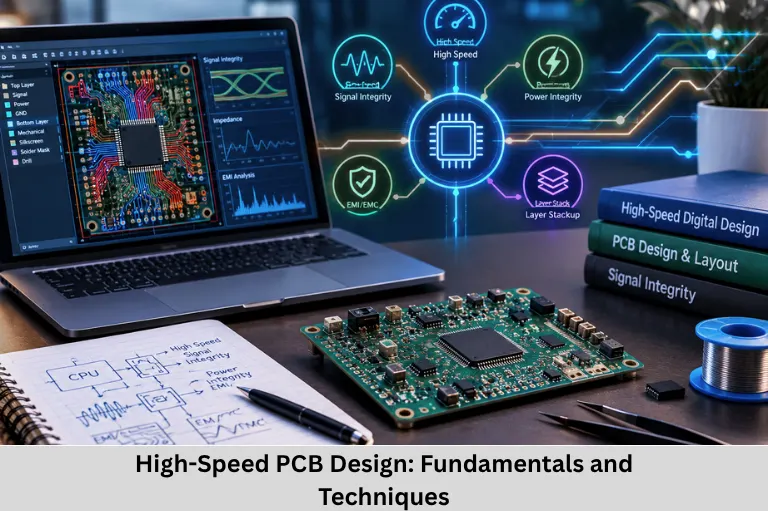
Learn high-speed PCB design, controlled impedance, signal integrity, crosstalk, PCB stack-up, differential routing, EMI/EMC and termination techniques. Embedded Tech Development Academy (ETDA).
- High-Speed PCB Design: Fundamentals and Techniques
- Introduction to High-Speed PCB Design: Fundamentals for Students and Professionals
Introduction to High-Speed PCB Design: Fundamentals for Students and Professionals
Introduction to High-Speed PCB Design
Modern electronic systems require higher data rates, faster switching signals, compact circuit layouts, and reliable communication between integrated circuits. These requirements make high-speed PCB design an essential part of digital electronics, embedded systems, telecommunications, automotive electronics, and computer hardware engineering.
High-speed printed circuit board (PCB) design focuses on maintaining signal integrity, controlled impedance, power integrity, timing accuracy, return-path continuity, and electromagnetic compatibility (EMC). Unlike low-speed circuits, high-speed designs must account for transmission-line behavior, parasitic capacitance, inductance, signal reflections, crosstalk, and electromagnetic interference (EMI).
A signal does not become high-speed solely because its clock frequency is high. Its rise time and fall time, combined with PCB trace propagation delay, determine when transmission-line effects become significant. A useful engineering guideline is to examine whether the signal edge time is comparable to or shorter than approximately twice the trace propagation delay.
High-speed design techniques are essential for interfaces such as USB, HDMI, PCI Express (PCIe), DDR memory, Ethernet, LVDS, MIPI, SPI, and RF circuits. Engineers must carefully select trace geometry, dielectric materials, layer stack-up, termination methods, and component placement to achieve reliable operation.
Embedded Tech Development Academy (ETDA) supports practical technical learning in embedded systems, electronics, hardware interfacing, and industry-relevant development skills. Learners seeking a Top Embedded Training Institute in Bangalore can strengthen their electronics foundation and explore hardware-oriented engineering topics with assured placement support.
High-Speed Interfaces and Buses
Common High-Speed Protocols
High-speed PCBs support interfaces that transfer digital information at high data rates or contain fast electrical transitions.
Digital Communication Interfaces
Common examples include:
- USB 2.0, USB 3.x and USB Type-C
- HDMI and DisplayPort
- Ethernet, including Gigabit Ethernet and 10 Gigabit Ethernet
- PCI Express and SATA
- DDR3, DDR4 and DDR5 memory
- LVDS and MIPI camera/display interfaces
- High-speed SPI and QSPI
- Wi-Fi, Bluetooth and other RF signal paths
Interface-Specific Requirements
Each interface has its own electrical specifications, impedance requirements, timing limits, and routing constraints. Designers must follow the applicable device datasheets and interface standards rather than applying one routing rule to every signal.
Key Design Considerations in High-Speed PCB Design
Controlled Impedance
Controlled impedance ensures that a PCB trace maintains a specified characteristic impedance based on its geometry and surrounding dielectric materials.
Trace Geometry and Materials
Trace width, copper thickness, dielectric constant, distance to the reference plane, and layer structure affect impedance.
Impedance Matching
Impedance discontinuities can produce reflections that distort signal edges. Controlled-impedance routing is particularly important for high-speed serial links, memory interfaces, and RF circuits.
Signal Integrity
Signal integrity describes how accurately an electrical signal reaches its destination.
Common Signal Problems
Reflections, attenuation, ringing, overshoot, undershoot, jitter, and noise can reduce signal quality.
Validation Techniques
Designers use oscilloscope measurements, time-domain reflectometry (TDR), simulation, and eye diagrams to evaluate signal behavior.
Crosstalk Reduction
Crosstalk occurs when electromagnetic coupling transfers unwanted energy between nearby traces.
Spacing and Routing
Increasing spacing between sensitive traces, minimizing long parallel runs, and routing adjacent signal layers in suitable directions can reduce coupling.
Reference-Plane Shielding
A continuous reference plane can reduce electromagnetic coupling when the stack-up and trace geometry are properly designed.
PCB Layer Stack-Up and Return Paths
Layer Stack-Up Design
A PCB stack-up defines the arrangement of signal, ground, and power layers.
Reference Planes
High-speed signals need a nearby, continuous reference plane to provide a low-inductance return path.
Preventing Return-Path Discontinuities
Splits, gaps, and abrupt changes in reference planes can force return currents onto longer paths, increasing loop inductance and EMI. Signal transitions between layers should be planned with suitable return-path vias.
Power Integrity
Power integrity ensures that integrated circuits receive stable supply voltages during switching activity.
Decoupling Capacitors
Decoupling capacitors provide local charge and help reduce power-distribution impedance across relevant frequency ranges.
Power Distribution Network
A robust power distribution network considers regulator response, plane impedance, capacitor placement, via inductance, and transient current demand.
Differential Pair Routing and Timing
Differential Signaling
Differential pairs use two related signals to communicate information. The receiver detects the voltage difference between the conductors.
Pair Geometry
Designers must control differential impedance, trace spacing, routing symmetry, and reference-plane continuity.
Skew Control
Length matching helps limit timing skew, but electrical matching also depends on dielectric properties, vias, and routing geometry. Length matching should follow the requirements of the specific interface.
Via and Stub Management
Vias introduce parasitic inductance and capacitance. Unused via stubs can create resonances and degrade high-frequency signal transmission.
Reducing Discontinuities
Minimize unnecessary layer transitions and use suitable via structures.
Back-Drilling
Back-drilling removes unused portions of plated through-hole vias when required by the signal-integrity budget.
EMI/EMC and Termination Techniques
Electromagnetic Compatibility
EMI can affect nearby circuits, wireless receivers, and sensitive analog components. EMC design aims to limit unwanted emissions and maintain immunity to external disturbances.
Practical EMI Reduction
Useful techniques include continuous reference planes, compact current loops, controlled edge rates where appropriate, proper grounding, filtering, and shielding.
Compliance Testing
Pre-compliance measurements and formal EMC testing help identify emissions and immunity problems before product release.
Signal Termination
Termination reduces reflections by matching the transmission-line environment to the source or load.
Common Termination Methods
- Series termination: A resistor near the driver helps match source impedance.
- Parallel termination: A resistor network near the receiver can match the line impedance.
- Differential termination: A resistor across a differential pair provides the specified differential load.
Choosing the Correct Method
Termination depends on driver characteristics, receiver requirements, topology, voltage levels, power consumption, and interface specifications.
High-Speed PCB Design Workflow
From Schematic to Validation
A reliable design process starts with electrical requirements and component selection before moving to PCB layout.
Design Steps
- Define interface speeds and timing constraints.
- Select stack-up and dielectric materials.
- Plan component placement and reference planes.
- Route critical signals using appropriate impedance rules.
- Verify power integrity and return paths.
- Run design-rule checks and signal-integrity simulations.
- Validate prototypes through measurement and testing.
Engineering Tools
PCB layout tools, impedance calculators, field solvers, signal-integrity simulators, and oscilloscopes help engineers evaluate the design before production.
Embedded Tech Development Academy (ETDA) encourages practical understanding of electronic hardware and embedded design concepts. A Top Embedded Training Institute in Bangalore should connect theoretical electronics knowledge with practical engineering methods and assured placement support.
Frequently Asked Questions
What is high-speed PCB design?
High-speed PCB design is the process of laying out circuit boards while accounting for transmission-line effects, signal timing, impedance, reflections, crosstalk, and electromagnetic interference.
Why is controlled impedance important?
Controlled impedance helps reduce signal reflections caused by impedance discontinuities and supports reliable signal transmission in high-speed circuits.
How can crosstalk be reduced?
Crosstalk can be reduced by maintaining appropriate trace spacing, limiting parallel routing, using continuous reference planes, and controlling stack-up geometry.
Why are ground planes important in high-speed PCBs?
Ground planes provide low-inductance return paths, support impedance control, and help reduce electromagnetic emissions when correctly designed.
Why is termination required in high-speed circuits?
Termination reduces reflections by matching the relevant source, transmission-line, or load impedance according to the circuit topology.
Conclusion
High-speed PCB design is essential for modern electronics that depend on fast signal transitions, high data rates, compact layouts, and reliable digital communication. Successful designs require engineers to understand signal integrity, controlled impedance, transmission-line theory, crosstalk, power integrity, differential pair routing, timing skew, return-path continuity, via stubs, EMI, and EMC.
The quality of a high-speed PCB depends on the relationship between electrical behavior and physical layout. Trace geometry, dielectric properties, copper thickness, layer stack-up, component placement, decoupling, and termination techniques all influence circuit performance. Engineers should combine sound layout practices with simulation and physical measurements to identify issues such as reflections, ringing, jitter, and excessive noise.
These technical concepts are particularly important for USB, HDMI, PCIe, DDR memory, Ethernet, MIPI, LVDS, RF circuits, and high-speed embedded systems. A strong understanding of PCB design rules, transmission-line effects, impedance matching, and validation techniques helps engineers develop hardware that is reliable, manufacturable, and compliant with relevant specifications.
Embedded Tech Development Academy (ETDA) supports practical technical learning in embedded systems, electronics, microcontrollers, and hardware development. Students looking for a Top Embedded Training Institute in Bangalore can build foundational skills that complement their understanding of PCB design, embedded hardware, and system integration, with assured placement support.
As electronic products continue to demand faster communication and greater integration, high-speed PCB design will remain a valuable engineering skill. Learners should develop the ability to interpret datasheets, understand interface specifications, select appropriate stack-ups, analyze signal paths, and validate hardware through simulation and measurement.
For students and professionals planning a career in embedded hardware, Embedded Tech Development Academy (ETDA) can support the development of practical technical knowledge. Choosing a Top Embedded Training Institute in Bangalore with hands-on learning and assured placement support can help learners connect electronics fundamentals with industry-oriented engineering skills.
Ultimately, high-speed PCB design is not simply about routing traces between components. It is about controlling how electrical energy travels through a physical structure. Mastering signal integrity, power integrity, impedance control, return paths, and EMI/EMC provides a strong foundation for developing dependable next-generation electronic systems.
Author: ETDA Trainers
Experience: 10+ Years of Industry Experience in Embedded Systems, IoT, and Embedded C Programming