
PCB Design: Process, Types, Tools & Modern PCB Manufacturing Guide
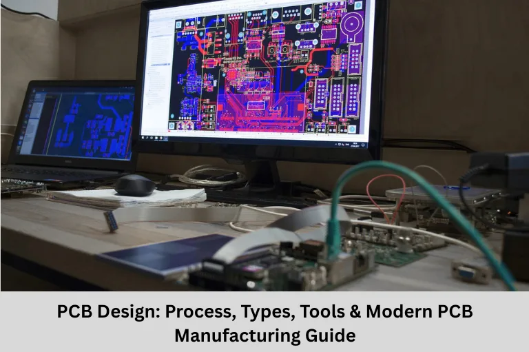
Learn PCB design fundamentals, design process, layout techniques, signal integrity, PCB tools, manufacturing, HDI technology, and future trends in electronics.
- PCB Design: Process, Types, Tools & Modern PCB Manufacturing Guide
- Introduction: Understanding PCB Design in Modern Electronics
Introduction: Understanding PCB Design in Modern Electronics
Printed Circuit Board (PCB) design is the foundation of virtually every electronic device we use today. Whether it’s a smartphone, laptop, smartwatch, industrial automation system, medical device, automotive control unit, or satellite communication equipment, every electronic product depends on a well-designed PCB to function reliably. PCB design transforms an electronic circuit from a schematic diagram into a physical board that connects electronic components through precisely engineered copper traces.
As electronics continue to become smaller, faster, and more powerful, PCB design has evolved into a highly specialized engineering discipline that combines electronics design, circuit layout, signal integrity, power integrity, thermal management, electromagnetic compatibility (EMC), and manufacturability. Modern PCB designers must consider not only the electrical performance of a circuit but also manufacturing processes, component availability, reliability, cost optimization, and environmental compliance.
The rapid advancement of technologies such as Artificial Intelligence (AI), Internet of Things (IoT), 5G communication, embedded systems, electric vehicles (EVs), robotics, aerospace electronics, industrial automation, wearable devices, and high-speed computing has significantly increased the demand for advanced PCB design techniques. Engineers today work with complex multilayer PCBs, High-Density Interconnect (HDI) boards, flexible circuits, RF PCBs, and high-speed digital layouts capable of supporting gigabit data rates.
Understanding concepts such as PCB layout design, schematic capture, PCB routing, multilayer PCB design, impedance control, differential pair routing, PCB fabrication, Gerber files, Design Rule Check (DRC), Design for Manufacturing (DFM), Design for Assembly (DFA), signal integrity analysis, and electronic design automation (EDA) is essential for students, electronics engineers, embedded developers, and hardware designers.
In this article, we’ll explore the complete PCB design process, important design considerations, modern PCB technologies, industry-standard software tools, current challenges, and future innovations shaping the electronics manufacturing industry.
What is PCB Design?
PCB (Printed Circuit Board) design is the process of creating the physical layout of an electronic circuit by arranging electronic components and routing conductive copper traces on a board.
The PCB acts as both the electrical and mechanical foundation of an electronic system.
Why PCB Design is Important
A well-designed PCB offers:
- Reliable electrical connections
- Compact circuit implementation
- High-speed signal transmission
- Reduced electromagnetic interference
- Improved thermal performance
- Easier manufacturing and assembly
The PCB Design Process
Designing a PCB involves several important stages.
1. Schematic Design
The first step is creating the electronic circuit using Electronic Design Automation (EDA) software.
Main Activities
- Circuit conceptualization
- Component selection
- Library management
- Electrical Rule Check (ERC)
Popular Schematic Design Software
- Altium Designer
- KiCad
- Autodesk Eagle
- Cadence OrCAD
2. PCB Board Layout
After completing the schematic, designers create the board layout.
Layout Activities
- Component placement
- Signal routing
- Layer stack-up design
- Design Rule Check (DRC)
Proper component placement significantly improves PCB performance and manufacturability.
3. Design Verification
Before manufacturing, the PCB design must be verified.
Verification Methods
- Signal Integrity (SI) Analysis
- Power Integrity (PI) Simulation
- Thermal Analysis
- EMI/EMC Verification
These simulations help identify potential design issues before fabrication.
4. Manufacturing Preparation
Once verified, manufacturing files are generated.
Manufacturing Documents
- Gerber Files
- NC Drill Files
- Pick-and-Place Files
- Assembly Drawings
- Bill of Materials (BOM)
These files are provided to PCB fabrication and assembly companies.
Key PCB Design Considerations
Successful PCB design requires balancing electrical, mechanical, and manufacturing requirements.
Signal Integrity
Signal integrity ensures reliable transmission of high-speed digital signals.
Best Practices
- Controlled impedance routing
- Differential pair matching
- Crosstalk reduction
- Via optimization
Power Delivery Network (PDN)
A stable power distribution system is essential for reliable circuit operation.
Important Techniques
- Power plane design
- Ground plane optimization
- Decoupling capacitor placement
- Voltage drop analysis
Thermal Management
Heat significantly affects electronic component reliability.
Thermal Design Methods
- Copper pour optimization
- Thermal vias
- Heat sink placement
- Thermal relief structures
Design for Manufacturing (DFM)
A PCB should be designed for easy manufacturing.
DFM Considerations
- Minimum trace width
- Via sizes
- Component spacing
- Solder mask clearance
- Panelization
Why DFM Matters
Following DFM guidelines reduces manufacturing defects and production costs.
Modern PCB Technologies
Modern electronic systems demand advanced PCB technologies.
High-Density Interconnect (HDI)
HDI PCBs use:
- Microvias
- Laser drilling
- Fine-pitch BGAs
- Sequential lamination
HDI technology enables compact and lightweight electronic products.
Flexible and Rigid-Flex PCBs
Flexible circuits are widely used in:
- Smartphones
- Medical devices
- Cameras
- Wearable electronics
Rigid-flex boards combine both rigid and flexible PCB sections.
High-Speed PCB Design
High-speed circuits require careful routing.
Important Techniques
- Low-loss PCB materials
- Controlled impedance
- Length matching
- Back-drilling
RF and Microwave PCB Design
RF PCBs are used in:
- Wireless communication
- Satellite systems
- Radar
- 5G infrastructure
PCB Design Software Tools
EDA software simplifies PCB development.
Industry Standard Tools
Popular tools include:
- Altium Designer
- Cadence Allegro
- Mentor Graphics PADS
- OrCAD
- Autodesk Eagle
Open-Source PCB Software
KiCad has become one of the most popular free PCB design tools.
Simulation Software
Design verification includes:
- Electromagnetic Simulation
- Thermal Modeling
- Signal Integrity Analysis
- Mechanical Simulation
Industry Challenges in PCB Design
Modern PCB engineers face numerous challenges.
Miniaturization
Electronic devices continue becoming smaller.
Challenges include:
- Tiny component packages
- Dense routing
- Limited board area
High-Speed Design Complexity
Modern processors require:
- DDR5 routing
- PCIe Gen5/Gen6 routing
- USB4
- HDMI 2.1
Supply Chain Issues
Component shortages require designers to:
- Select alternate parts
- Manage component lifecycle
- Reduce redesign costs
Environmental Compliance
Modern PCBs must comply with:
- RoHS
- REACH
- Lead-free manufacturing
Future Trends in PCB Design
PCB technology continues evolving rapidly.
Embedded Components
Passive and active components are increasingly embedded inside PCB layers.
Advanced PCB Materials
New materials provide:
- Better thermal conductivity
- Lower dielectric loss
- Higher reliability
AI-Assisted PCB Design
Artificial Intelligence is helping engineers with:
- Auto-routing
- Component placement
- DRC optimization
- Failure prediction
3D Printed Electronics
Additive manufacturing enables:
- Printed conductive traces
- Rapid prototyping
- Hybrid electronics manufacturing
Future Outlook
Technologies like AI-driven PCB layout, embedded electronics, flexible PCBs, advanced semiconductor packaging, chiplet integration, high-speed computing, electric vehicles, Internet of Things (IoT) devices, and aerospace electronics will redefine PCB manufacturing over the next decade.
Frequently Asked Questions (FAQs)
What is PCB design?
PCB design is the process of creating the physical layout of an electronic circuit by placing components and routing electrical connections on a printed circuit board.
Which software is commonly used for PCB design?
Popular PCB design software includes Altium Designer, Cadence Allegro, OrCAD, KiCad, Autodesk Eagle, and Mentor Graphics PADS.
What is the purpose of Design Rule Check (DRC)?
Design Rule Check (DRC) verifies that the PCB layout follows manufacturing and electrical design rules, helping prevent errors before fabrication.
What is High-Density Interconnect (HDI) PCB technology?
HDI PCB technology uses microvias, fine-pitch components, and multilayer designs to create compact, high-performance circuit boards for modern electronic devices.
Why is signal integrity important in PCB design?
Signal integrity ensures that high-speed electrical signals travel across the PCB without distortion, noise, crosstalk, or timing issues, improving the reliability and performance of electronic systems.
Conclusion
PCB design serves as the bridge between innovative electronic ideas and real-world products. By combining schematic design, PCB layout, signal integrity, power integrity, thermal management, multilayer PCB technology, high-speed routing, PCB fabrication, and electronics manufacturing, engineers create reliable and high-performance electronic systems used across every industry.
From consumer electronics and embedded systems to automotive electronics, medical equipment, aerospace, industrial automation, robotics, telecommunications, and defense applications, PCB technology remains an indispensable part of modern engineering. As devices continue becoming faster, smaller, and more intelligent, PCB designers must master advanced concepts such as HDI PCB design, impedance control, RF PCB layout, differential routing, Design for Manufacturing (DFM), Design for Assembly (DFA), and Electronic Design Automation (EDA).
The future of PCB design is being shaped by Artificial Intelligence (AI), 3D printed electronics, embedded components, flexible circuits, chiplet architectures, advanced PCB materials, sustainable manufacturing, and automated design optimization. Engineers who develop expertise in these emerging technologies will play a key role in driving the next generation of electronic innovation.
Whether you’re an electronics student, embedded systems engineer, hardware designer, or PCB layout professional, mastering PCB design fundamentals is essential for building reliable, efficient, and manufacturable electronic products.
Author: ETDA Trainers
Experience: 10+ Years of Industry Experience in Embedded Systems, IoT, and Embedded C Programming